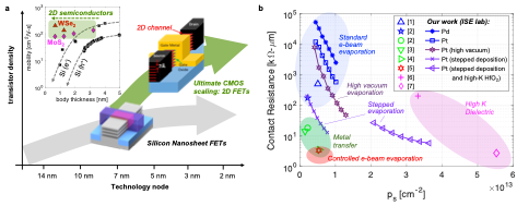
With the advent of semiconducting 2D transition metal dichalcogenides (TMDs), field-effect transistors (FETs) can be scaled down even further, offering promising possibilities for retaining Moore's law (Figure 1a). Conventionally, bulk semiconductors are used in the channel of standard CMOS technology, but these cannot be scaled below 5 nm in thickness without posing substantial problems relating to variance, surface roughness, and dangling bonds, which reduce charge carrier mobility (Figure 1a, inset). However, using 2D semiconductors (such as TMDs), which maintain their desirable electronic properties even at the limit of a single atomic layer (i.e., monolayer with thickness 1 nm), it is possible to fabricate sub-10 nm channel length FETs with well-controlled electrostatics and suitable mobilities. Since complementary n-type and p-type transistors are used in CMOS technology to accomplish logic functions, both n-type and p-type MOS transistors are required to scale CMOS technology to its optimum capability with 2D materials. While substantial efforts have been dedicated to improving 2D NMOS devices (e.g., using MoS2 semiconducting channels), the performance of 2D PMOS FETs has fallen behind. Research at the Ivan Sanchez Esqueda laboratory (ISE lab) conducted by PhD student Naim Patoary explores improvements in ultrascaled 2D WSe2 p-type MOS transistors with emphasis on contact resistance and its role in device performance. This work analyzed WSe2 FETs with few nm high-K metal-gate (HKMG) stacks and prepared using various methods aimed at improving contact resistance (Figure 1b). Significant improvements in performance benchmarks (e.g., on-state current vs. sub-threshold swing, Figure 2) were observed against the best published results indicating a promising path towards the ultimate scaling of CMOS technology using 2D materials.
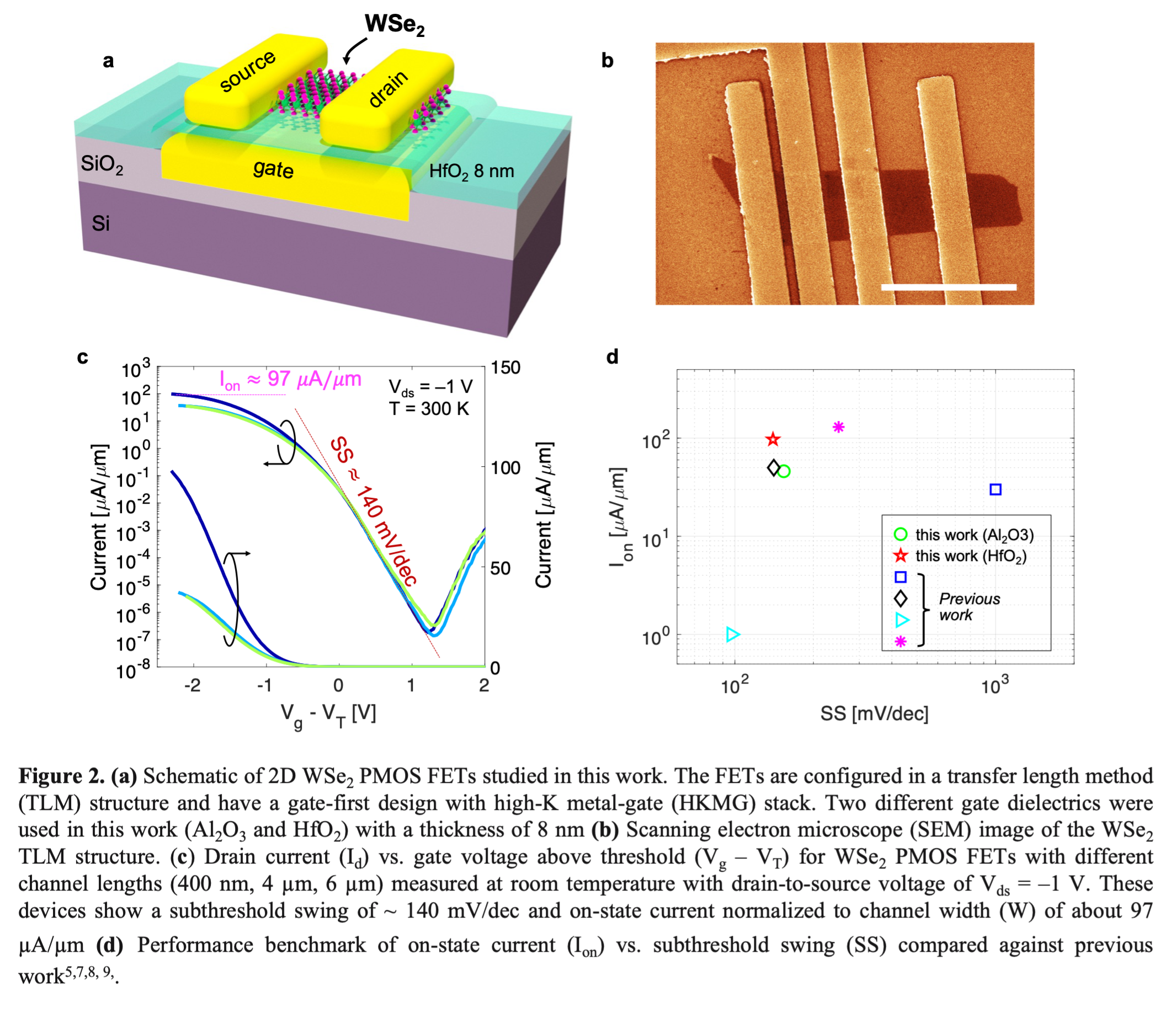
Our work prepared p-type transistors with few layer (3-5 layer) WSe2 channels. These are designed and fabricated with a high-K metal-gate (HKMG) stack featuring 8 nm of either Al2O3 or HfO2 gate dielectrics. High work function (WF) metal contacts were used to facilitate the injection and conduction of positively charged carriers (holes) into the WSe2 channels. A 3D schematic of the test structure is shown in Figure 2a.
Our gate-first HKMG process includes patterning and deposition of a Cr/Au metal gate (e-beam lithography, evaporation, and lift-off) followed by atomic-layer deposition (ALD) of the high-K dielectric (8 nm Al2O3 or HfO2). Electron beam lithography was conducted using the JEOL 6000FS at the NanoFab ASU facility to define a transfer-length method (TLM) pattern of source and drain electrodes using PMMA (Polymethyl methacrylate) as mask (SEM image of TLM structure shown in Figure 2b). The metals (Pt/Au or Pd/Au) were deposited by e-beam metal evaporation (Lesker 3) in the cleanroom facility at a rate of 2 Å/s at a pressure of 10-7 torr to ensure the uniformity of the electrode pads. Our study reports low contact resistance ~5.7 kΩ-µm, with on-state currents of ~97 µA/µm and subthreshold swing of ~140 mV/dec in FETs with channel lengths of 400 nm (Figure 2c,d). Apart from providing significant insights on emerging methods to enhance contact quality and improve performance of p-type FETs with 2D channel materials, our work presented physics-based model calculations for ballistic WSe2 devices to elucidate the performance of extremely scaled FETs towards the ultimate limit of CMOS scaling.
References
1. Jung, D. H., Kim, S. il & Kim, T. W. Characteristics of electrical metal contact to monolayer WSe2. Thin Solid Films 719, (2021).
2. Zhang, X. et al. Molecule-Upgraded van der Waals Contacts for Schottky-Barrier-Free Electronics. Advanced Materials 33, (2021).
3. Kong, L. et al. Doping-free complementary WSe2 circuit via van der Waals metal integration. Nat Commun 11, (2020).
4. Jung, Y. et al. Transferred via contacts as a platform for ideal two-dimensional transistors. Nat Electron 2, 187–194 (2019).
5. Wang, Y. et al. P-type electrical contacts for 2D transition-metal dichalcogenides. Nature (2022) doi:10.1038/s41586-022-05134-w.
6. Dorow, C. J. et al. Advancing Monolayer 2D NMOS and PMOS Transistor Integration From Growth to van der Waals Interface Engineering for Ultimate CMOS Scaling. Nano Lett vol. 1 (2019). 7. O’Brien, K. P. et al. Advancing 2D Monolayer CMOS Through Contact, Channel and Interface Engineering. in Technical Digest - International Electron Devices Meeting, IEDM vols 2021-December
7.1.1-7.1.4 (Institute of Electrical and Electronics Engineers Inc., 2021).
8. Cheng, C. C. et al. First demonstration of 40-nm channel length top-gate WS2 pFET using channel area-selective CVD growth directly on SiOx/Si substrate. Dig. Tech. Pap. - Symp. VLSI Technol. 2019-June, T244–T245 (2019).
9. Li, K. S. et al. MoS2 U-shape MOSFET with 10 nm channel length and poly-Si source/drain serving as seed for full wafer CVD MoS2 availability. Dig. Tech. Pap. - Symp. VLSI Technol. 2016-September, 2015–2016 (2016).
Authors: Md Naim Patoary and Dr. Ivan Sanchez Esqueda