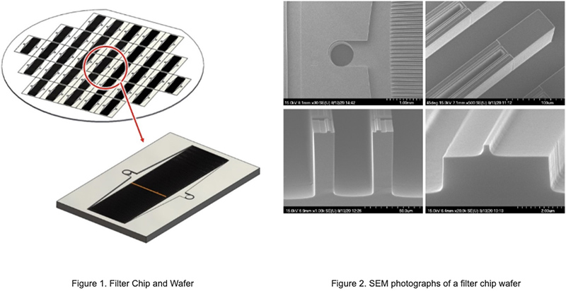
As part of the collective effort to control and mitigate the spread of COVID-19, a variety of research groups at ASU are working together to develop a rapid and highly accurate test for the detection of SARS-CoV-2 in human saliva. The first component of this test is a combined silicon and glass filter that is used to remove constituents of saliva that are larger than the virus itself. This is accomplished by etching sets of ridges into the silicon substrate to a depth that is slightly larger than the known diameter of SARS-CoV-2. Then, a glass substrate is bonded to the silicon such that it forms a “ceiling” above the ridge which creates the necessary nanoscale gaps that perform the filtration. This filtration process effectively concentrates the virus and prepares it for the genetic detection component of the test that is very specific for SARS-CoV-2. The result is the creation of a test that is non-invasive, affordable, easily repeatable, more sensitive than the standard nasopharyngeal swab test, field-deployable, and operates on the scale of minutes instead of hours or days.
Fabrication of the filter chip wafers is accomplished in the Arizona State University NanoFab. The NanoFab is a flexible nanoscale processing and fabrication facility offering state-of-the-art device processing and characterization tools for university research and external company prototype development. Core strengths are nanofabrication, unique silicon processing, molecular- and bioelectronics, microelectromechanical systems, nano-fluidics, optoelectronics and device characterization. The expertise of the skilled NanoFab staff, several of whom have more than 25 years of experience, is also available to users.
The entire filter chip fabrication process is integrated in the NanoFab. A series of photolithography and etch steps are performed using a 3c Technical GCA wafer stepper, and an SPTS Technologies multiplexing deep silicon etcher.
The SPTS system is designed to etch deep, highly anisotropic, high aspect ratio patterns in silicon using a time multiplexed process that is typically referred to as the “Bosch” process. This process utilizes a cyclic etch/passivation scheme to etch deep, highly anisotropic patterns in silicon. The etch cycle is typically performed with an SF6 plasma, and the passivation cycle is typically performed with a C4F8 plasma. The filter chip requires etch depths that are both shallow (< 1 μm) and very deep (> 400 μm). The SPTS system is used in both multiplexed, and non-multiplexed mode to perform these varied etches, including an etch that goes completely through a 400 μm thick silicon wafer.
The demands of the filter chip on the etch processes also extend to the photolithography processes used to define the etch patterns. One photolithography process must produce submicron (~0.6 μm) patterns. Another photolithography process must be able to mask the 400 μm through silicon via etch. A third photolithography process must be able to mask a 100 μm deep which while simultaneously covering 4 μm steps that have already been etched into the silicon. Each of these processes presents different challenges that must be overcome in different ways.
After wafer processing, the completed silicon wafer is anodically bonded to a sheet of borosilicate glass, known as the “cover glass”. The bonding processes produces a rugged, durable bond. Either the silicon wafer, or the borosilicate cover glass will break before the bond fails. The bonded silicon/glass pair is then diced using a conventional dicing saw to produce the individual filter chips.
The Hayes Research Group and the NanoFab plan to continue their collaboration in the fight against SARS-CoV-2. Planning for the next, more advanced separation filter is in progress, with fabrication expected to commence in the next few weeks.

