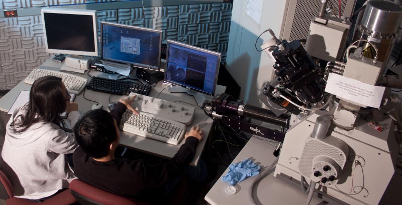
SEM/FIB Focused Ion Beam - Nova 200 NanoLab (FEI)

Description

The Nova NanoLab brings advanced capabilities and flexibility to researchers and developers needing to create, modify, and characterize complex structures below 100 nanometers. It combines ultra-high resolution field emission scanning electron microscopy (SEM) and precise focused ion beam (FIB) etch and deposition to complement your existing Nanotechnology laboratory tools and extend your applications range for nanoscale prototyping, machining, 2D and 3D-characterization, and analysis.

It comes equipped with integrated 3D-characterization and nano-machining, and nano-analysis. It is also capable of comprehensive beam chemistries for deposition and etch. Some typical nanotechnology applications are:

  • TEM sample preparation
  • Nanotube-based nano-structure assembly
  • Nano-bridge creation
  • Photonic array prototyping
  • Laser prototyping
  • Nano-stamping
  • AFM tip modification
  • MEMS modification

Nova NanoLab enables characterization of these structures via several methods, among them slice and view for 3D-reconstruction, ultra-high resolution in-lens backscattered electron imaging for phase contrast characterization, secondary ion imaging for grain contrast, and SPI- simultaneous patterning and imaging mode for real-time imaging feedback on the milling process.

Electron Optics

  • High-resolution Field Emission-SEM column, with monopole magnetic immersion final lens, Schottky thermal field emitter, 60 degree objective lens geometry and heated objective apertures.
  • Resolution @ optimum WD
    • 1.1 nm @ 15 kV (TLD-SE)
    • 2.5 nm @ 1 kV (TLD-SE)
    • 3.5 nm @ 500V TLD-SE
    • 5.5 nm @ 500 V TLD-BSE
  • Resolution @ beam coincidence point
    • 1.0 nm @ 30 kV STEM
    • 1.5 nm @ 15 kV (TLD-SE)
    • 2.0 nm @ 5 kV (TLD-SE)
  • Max. Horizontal field width: 3.0 mm at beam coincidence point (corresponds to 35x minimum magnification in quad view) 
  • Accelerating voltage: 200 V – 30 kV
  • Probe current: <= 20 nA in 21 steps

Detectors

  • ETD--Everhart-Thornley Detector for detecting secondary electrons, backscattered electrons, with additional custom capabilities.
  • TLD-Through the Lens Detector for detecting secondary electrons, backscattered electrons, with additional custom capabilities.

Digital image processor

  • Dwell: 50 ns - 1 ms
  • 11 presets + photo + snapshot
  • Up to 3584 x 3094 pixel resolution
  • File type: TIFF (8 or 16 bit), BMP or JPEG
  • Single frame or 4-quadrant image display
  • 4 quadrants live
  • up to 256 frame averaging or integration

Tools for Nano-prototyping

  • Ion Optics
    • Magnum™ ion column with Ga liquid metal ion source
    • Resolution: 7 nm (5 nm achievable)
    • Max. Horizontal field width: 2.5 mm at 5 kV and beams coincidence point (corresponds to 50x minimum magnification in quad view)
    • Accelerating voltage: 5 – 30 kV
    • Probe current: 1 pA – 20 nA in 15 steps
    •  Beam blanker standard – external control possible
    • 15 position aperture strip
  • Fabrication and machining
    • Minimum deposited line width (Ion beam, Pt): 50 nm achievable
    • Minimum deposited line width (Electron beam, Pt): 20 nm
    • Minimum etched line width (Si): ~50 nm achievable
    • Maximum hole aspect ratio (Si, 500 nm hole radius): 10:1
    •  Typical TEM sample prep membrane thickness: 50 - 100 nm (30 - 50 nm achievable)
  • Digital pattern generator
    • 4 k x 4 k resolution
    • 1 M pixels addressable
    •  Min. dwell: 100 ns o Max. dwell: 4 ms
  • Gas chemistry
    •  “Zero-collision” GIS design concept
      • Individual gas injectors with separate injections systems reconfigurable in the future
      • 5 µm placing accuracy without user interaction
    • Gas chemistry options
      •  Platinum metal deposition
      • Carbon deposition

Access Policies

Policies and Procedures for Access, Development and Maintenance

The FEI Nova 200 Dual-Beam FIB has been acquired under the NSF Major Research Instrumentation Program, with additional support from Arizona State University. This instrument will be made available to the ASU and broader community as a user facility, and should facilitate a wide range of applications involving the fabrication of nanostructures. No radioactive samples, and the sample must survive in a vacuum and under the electron beam.

Contact

Ken Mossman
Research Specialist
kenneth.c.mossman@asu.edu
480.965.0946

Techniques
  • Focused ion beam and sample preparation
Documents and manuals
ASU Unit
Knowledge Enterprise
Rates
Cost for ASU Internal Cost for ASU Internal with Staff Assistance Cost for Other Academic/Non-Profit Cost for Other Academic/Non-Profit with Staff Assistance
$66/h
$105/hr
$136/h
$224/h
Photos
Focused ion beam
Videos