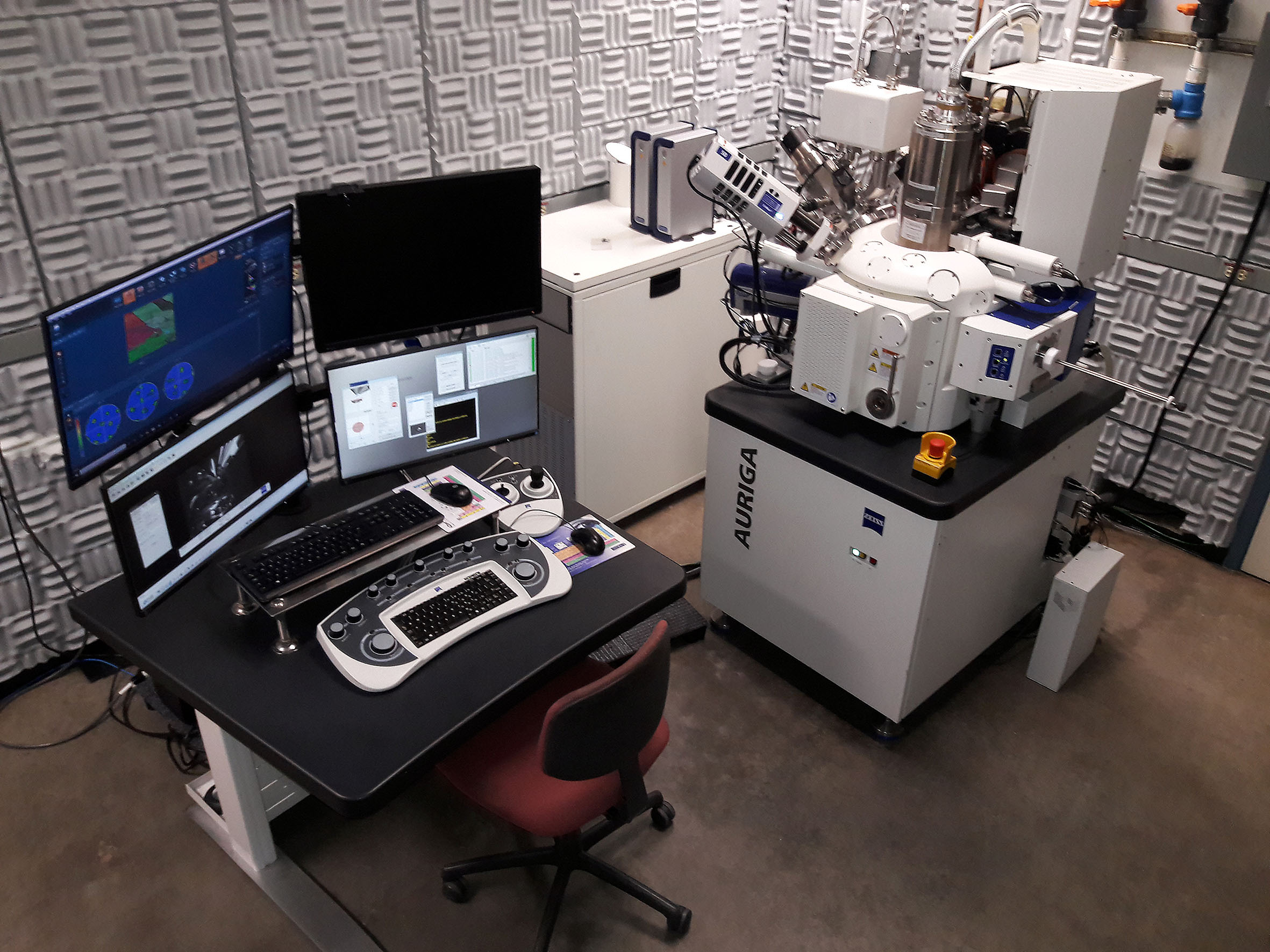
The Zeiss Auriga brings top-of-the-line capabilities and flexibility to researchers and developers combining high-resolution field emission scanning electron microscopy (SEM) and precision focused ion beam (FIB) etch and deposition. It complements your existing Nanotechnology laboratory tools and extends your application range for nanoscale prototyping, machining, 2D and 3D characterization, and analysis.
It comes equipped with integrated 3D characterization, visualization, and nano-machining. It is also capable of platinum deposition, automation, along with nano-analysis. Some typical nanotechnology applications are:
- Nanotube-based nano-structure assembly
- Nano-bridge creation
- Photonic array prototyping
- Laser prototyping
- Nano-stamping
- AFM tip modification
- MEMS modification
The Auriga enables characterization of these structures via several methods, among them slice and view for 3D-reconstruction, backscattered electron imaging for phase-contrast characterization, as well as secondary ion imaging for grain contrast.
Electron optics
- High-resolution Gemini Field Emission-SEM column, with Schottky thermal field emitter.
- Resolution @ optimum WD
- 1.0 nm @ 15 keV
- 1.9 nm @ 1 keV
- Accelerating voltage: 100 eV – 30 keV
- Probe current: 4pA – 20nA
Detectors
- Chamber -Everhart-Thornley Detector for detecting secondary electrons.
- In-lens- High-efficiency annular type for detecting secondary electrons.
- EsB – In-Column detector with filtering grid for detecting backscattered electrons.
- Oxford X-Max – An Energy Dispersive X-ray Spectrometer (EDS) that can be used to analyze the atomic composition of a sample with 50mm window capable of 129eV resolution.
- Oxford symmetry S2 EBSD detector (What is EBSD?)
Tools for Nano-prototyping
- Ion Optics
- Orsay Physics “Cobra” ion column with Ga liquid metal ion source
- Resolution: 2.5 nm at 30kV
- Accelerating voltage: 1kV – 30 kV
- Probe current: 1 pA – 20 nA
- Beam blanker standard – external control possible
- Digital pattern generator
- 2 k x 2 k resolution
- Min. dwell: 100 ns
- Max. dwell: 4 ms
- Gas chemistry
- Platinum metal deposition
Contact
Sisouk Phrasavath
Engineer Principal
sisouk.phrasavath@asu.edu
480.965.9153
Ken Mossman
Research Specialist
kenneth.c.mossman@asu.edu
480.965.0946
For EBSD
Axel Wittmann
Associate Research Scientist
Axel.Wittmann@asu.edu
480.727.8732
- SEM
- FIB
- EBSD
- EDS
| Cost for ASU Internal | Cost for ASU Internal with Staff Assistance | Cost for Other Academic/Non-Profit | Cost for Other Academic/Non-Profit with Staff Assistance |
|---|---|---|---|
|
$76.44/h
|
$119.49/h
|
$162.96/h
|
$259.56/h
|