Description
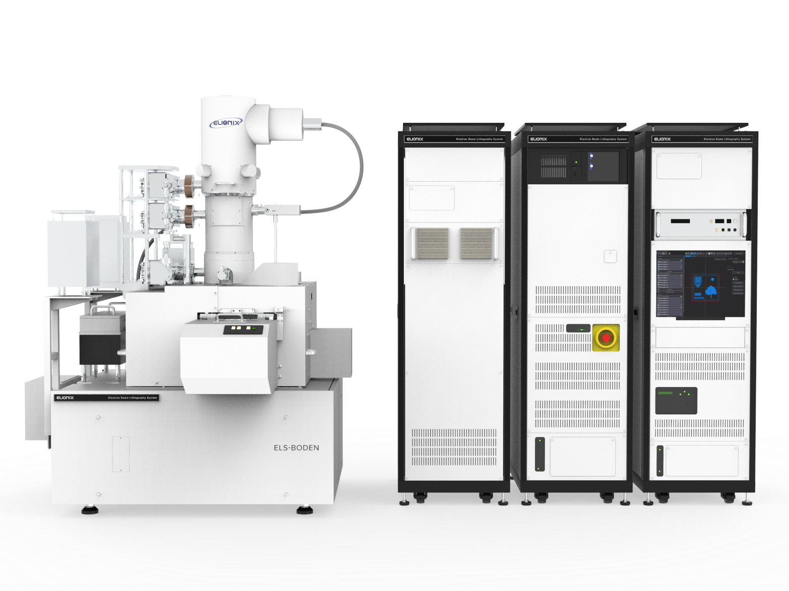
The Elionix ELS-BODEN 100keV Electron Beam Exposure System is available for high resolution lithography requirements.
Specs:
Accelerating voltage: 100 keV
Minimum beam diameter: 1.8nm
Minimum pixel size: 0.2nm
Field size: up to 1mm x 1mm
Resolution: 6 nm
Pattern format: GDS (DXF, DWG convertible with offline software Elionix CONV and GeniSys BEAMER)
Substrate:
- Two Piece part chucks
- 2" to 8” wafer chuck
Learn more about lithography deposition technique and associated tools.
Training:
Contact Kevin Nordquist for more information.
Techniques
- Lithography
ASU Unit
Knowledge Enterprise
Rates
| Service | ASU Internal Rate | External Organization Rate | Notes |
|---|---|---|---|
| Equipment use | $63/ Hour | Contact NanoFab |
Photos