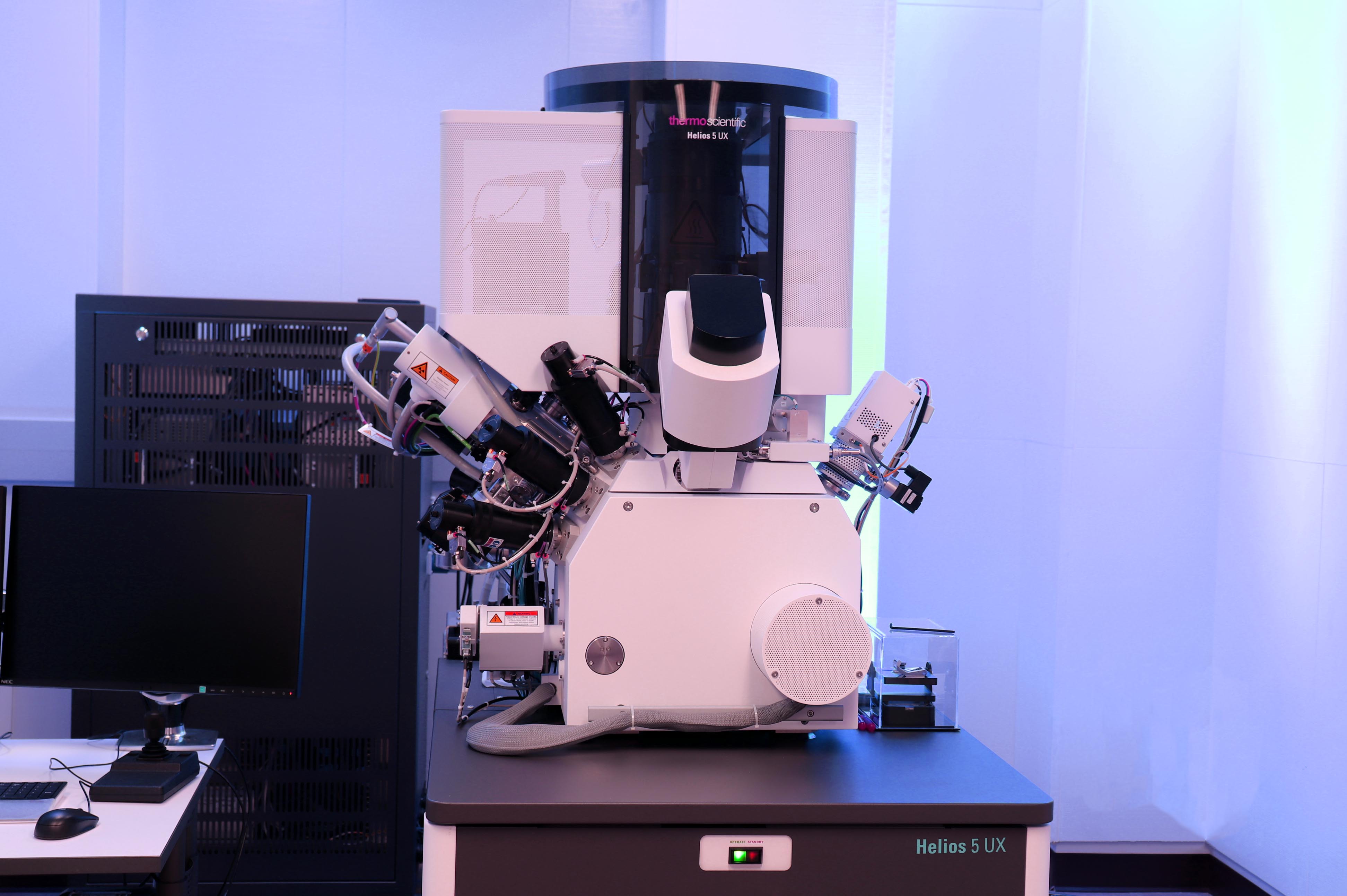
The Helios 5UX (Installation completed June 2020) brings cutting edge capabilities and flexibility to researchers and developers needing to create, modify, and characterize complex structures below 100 nanometers. It combines ultra-high resolution field emission scanning electron microscopy (SEM) and precise focused ion beam (FIB) etch and deposition to complement your existing Nanotechnology laboratory tools and extend your application range for nanoscale prototyping, machining, 2D and 3D-characterization, and analysis.
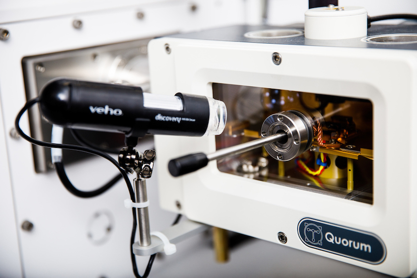
Quorum Cryo stage.
It comes equipped with integrated 3D-characterization, visualization, and nano-machining. It is also capable of comprehensive beam chemistries for deposition and etches, and automation, along with nano-analysis. Some typical nanotechnology applications are:
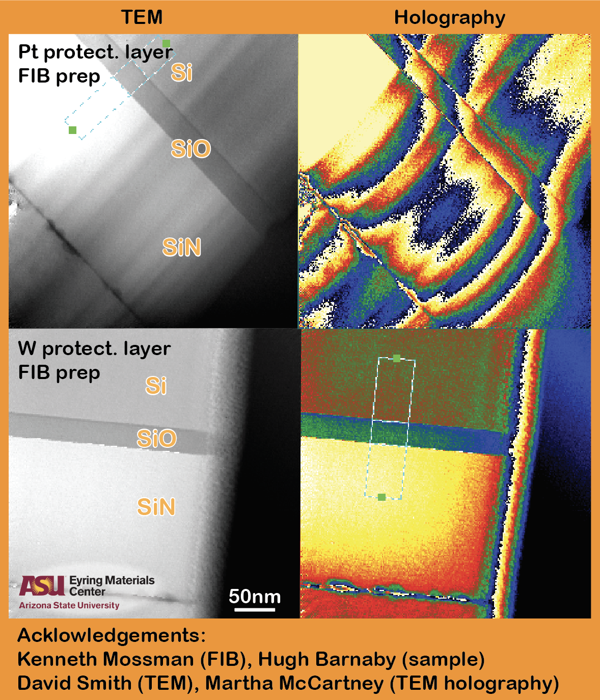
- Aberration-Corrected TEM sample preparation
- Nanotube-based nano-structure assembly
- Nano-bridge creation
- Photonic array prototyping
- Laser prototyping
- Nano-stamping
- AFM tip modification
- MEMS modification
The Helios 5UX enables characterization of these structures via several methods, among them slice and view for 3D-reconstruction, ultra-high-resolution in-lens backscattered electron imaging for phase-contrast characterization, secondary ion imaging for grain contrast, SPI- simultaneous patterning and imaging mode for real-time imaging feedback on the milling process, and STEM for sub-1 nm characterization.
Electron Optics
- High-resolution Field Emission-SEM column, with monopole magnetic immersion final lens, Schottky thermal field emitter, 60-degree objective lens geometry, and heated objective apertures.
- Resolution @ optimum WD
- 0.6 nm @ 2keV (TLD-SE)
- 0.7 nm @ 1 keV (TLD-SE)
- 1.0 nm @ 500eV TLD-SE
- 5.5 nm @ 500 V TLD-BSE
- Resolution @ beam coincidence point
- 1.0 nm @ 30 kV STEM
- 1.5 nm @ 15 kV (TLD-SE)
- 2.0 nm @ 5 kV (TLD-SE)
- Max. Horizontal field width: 3.0 mm at beam coincidence point (corresponds to 35x minimum magnification in quad view)
- Accelerating voltage: 200 eV – 30 keV
- Landing voltage: 20 eV – 30KeV
- Probe current: <= 100nA in 21 steps
Detectors
- ETD--Everhart-Thornley Detector for detecting secondary electrons, backscattered electrons, with additional custom capabilities.
- TLD-Through the Lens Detector for detecting secondary electrons, backscattered electrons, with additional custom capabilities.
- iCD – In-Column Detector for detecting backscattered electrons
- MD - Mirror Detector for detecting backscattered electrons
- ICE – Ion Conversion and Electron – for detecting secondary electron and secondary ion
- DBS – Directional Back -Scatter – for detecting backscattered electrons
- STEM 3+ - Scanning Transmission Electron Mode detector for detecting electrons transmitted through the sample.
- Octane Elect Super – Energy-Dispersive X-ray detector for elemental analysis
Digital image processor
- Dwell: 50 ns - 1 ms
- 11 presets + photo + snapshot
- Up to 3584 x 3094 pixel resolution
- File type: TIFF (8 or 16 bit), BMP or JPEG
- Single frame or 4-quadrant image display
- 4 quadrants live
- 256 frame average or integration
Tools for Nano-prototyping
- Ion Optics
- Phoenix™ ion column with Ga liquid metal ion source
- Resolution: 2.5 nm (using selective edge method)
- Max. Horizontal field width: 2.5 mm at 5 kV and beams coincidence point (corresponds to 50x minimum magnification in quad view)
- Accelerating voltage: 5 – 30 kV
- Probe current: 0.1 pA – 65 nA in 15 steps
- Beam blanker standard – external control possible
- Fabrication and machining
- Minimum deposited line width (Ion beam, Pt): 50 nm achievable
- Minimum deposited line width (Electron beam, Pt): 20 nm
- Minimum etched line width (Si): <15 nm achievable
- Maximum hole aspect ratio (Si, 500 nm hole radius): 10:1
- Maximum hole aspect ratio (Si, 500 nm hole radius, XeF2, coaxial needle): 20:1
- Typical TEM sample prep membrane thickness: 50 - 100 nm (30 - 50 nm achievable)
- Digital pattern generator
- 4 k x 4 k resolution
- 1 M pixels addressable
- Min. dwell: 100 ns o Max. dwell: 4 ms
- Gas chemistry
- “Zero-collision” GIS design concept
- Individual gas injectors with separate injections systems reconfigurable in the future
- 5 µm placing accuracy without user interaction
- Gas chemistry options
- Platinum metal deposition
- Carbon deposition
- Tungsten deposition
- Insulator deposition
- Selective Carbon Mill
- “Zero-collision” GIS design concept
Contact
Ken Mossman
Research Specialist
kenneth.c.mossman@asu.edu
480.965.0946
- Focused ion beam and sample preparation