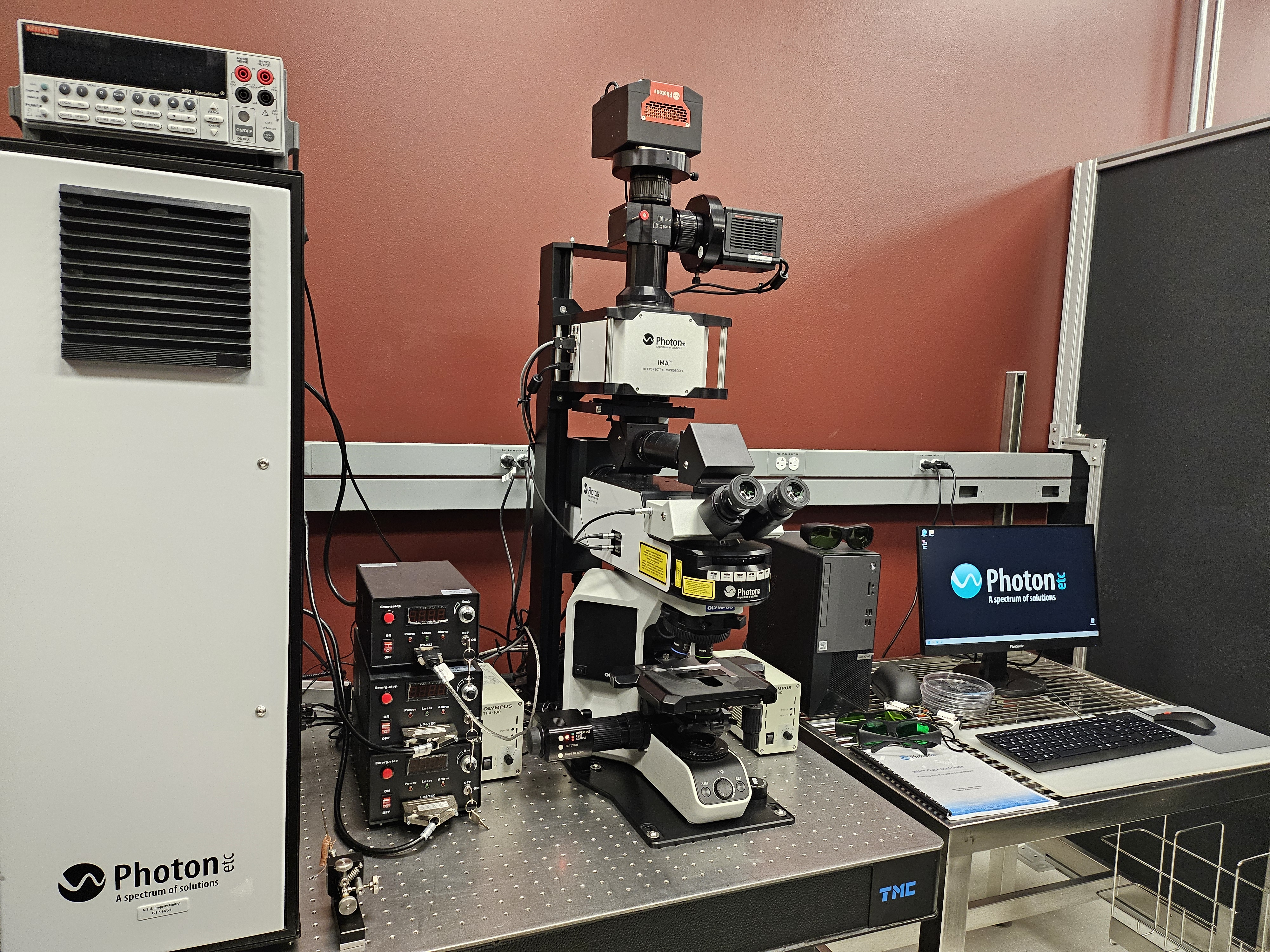
The hyperspectral imager provides spatial and spectral information, where each pixel of the field of view returns a spectrum. This technique can help map the sample composition, give feedback on its formation, identify defects, inhomogeneity, as well as fundamental physical properties such as photoluminescence, electroluminescence, fluorescence, and other optoelectronic properties.
This imaging system can be used to characterize materials from different families; organic, inorganic and hybrid semiconductors, carbon-based nanomaterials including fullerenes, carbon nanotubes, graphene and its derivatives, graphene oxide, nanodiamonds, and carbon-based quantum dots, perovskites and silicon-based materials. Moreover, this platform can also be used for the characterization of optoelectronic devices, for instance: photovoltaic solar cells, light emitting diodes, sensors and transistors. Additionally, it can be used for other kinds of samples for biological and life sciences applications.
Applications
- Perform complex material analyses such as solar cell characterization, nanomaterials, and semiconductor quality control by means of hyperspectral microscopy (PL, EL).
- Study novel IR markers in complex environments including live cells and tissue through the hyperspectral microscope.
- Advantage of a darkfield hyperspectral microscope to reveal nanoparticle properties on transparent, unstained samples, such as polymers, crystals, and living cells.
Please submit proof of completion of completion of EHS Laser Safety Training (EHS Laser Safety Train Course Link) prior to submitting a training request for the hyperspectral imager. Please download and read the Laser Safety manual here: ASU Laser Safety Manual_2023.pdf
| Service | ASU rate | Nonprofit/other academic rate | Industrial/ Private | Notes |
|---|---|---|---|---|
| Equipment Use | $44/ hour | $55/ hour | Please contact AEPCore@asu.edu |