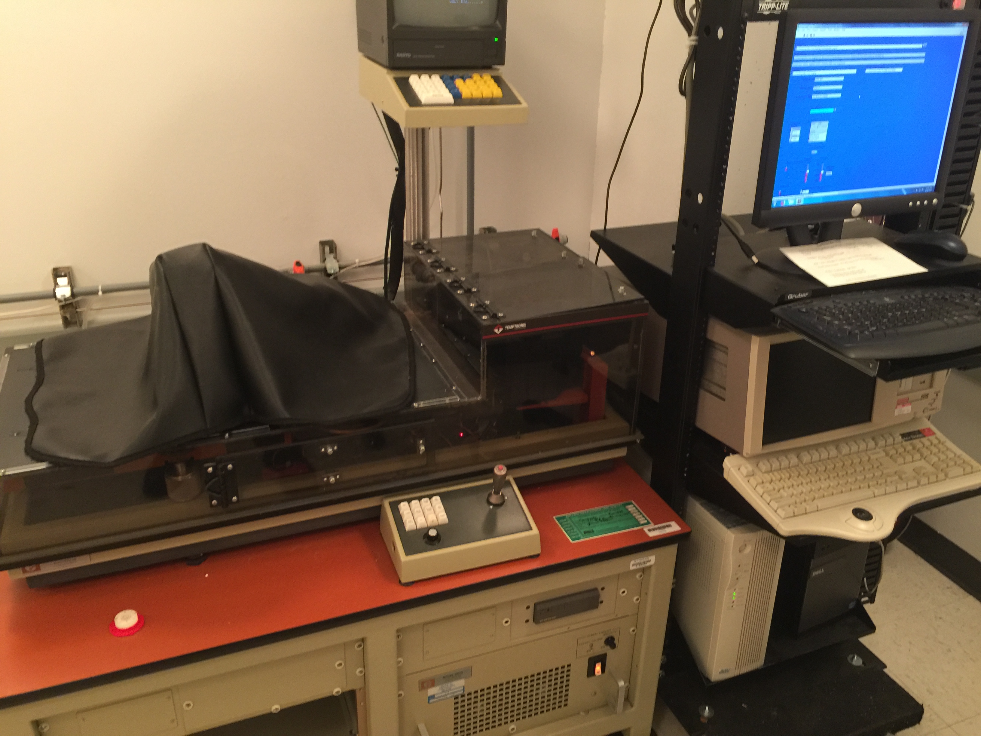
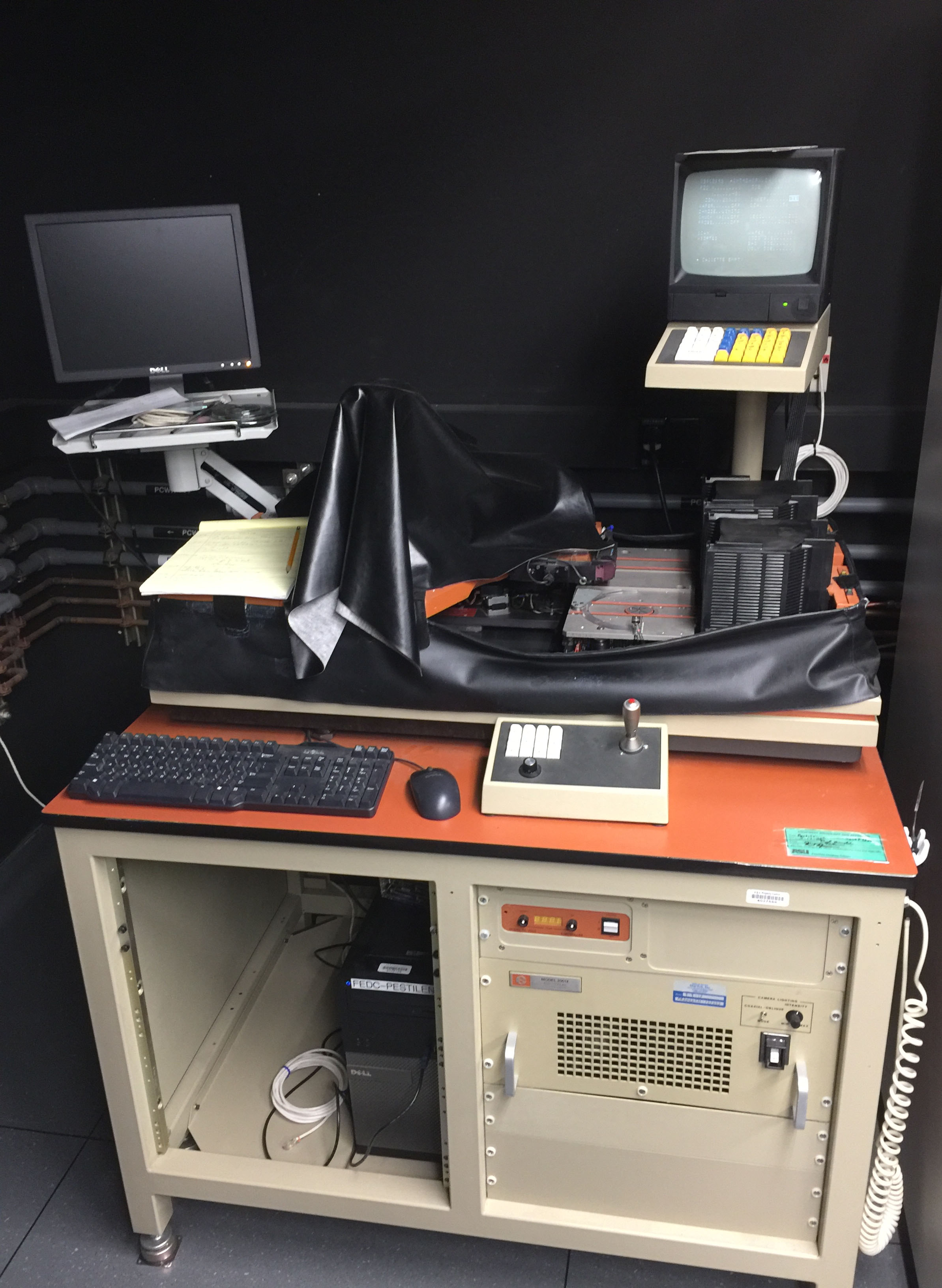
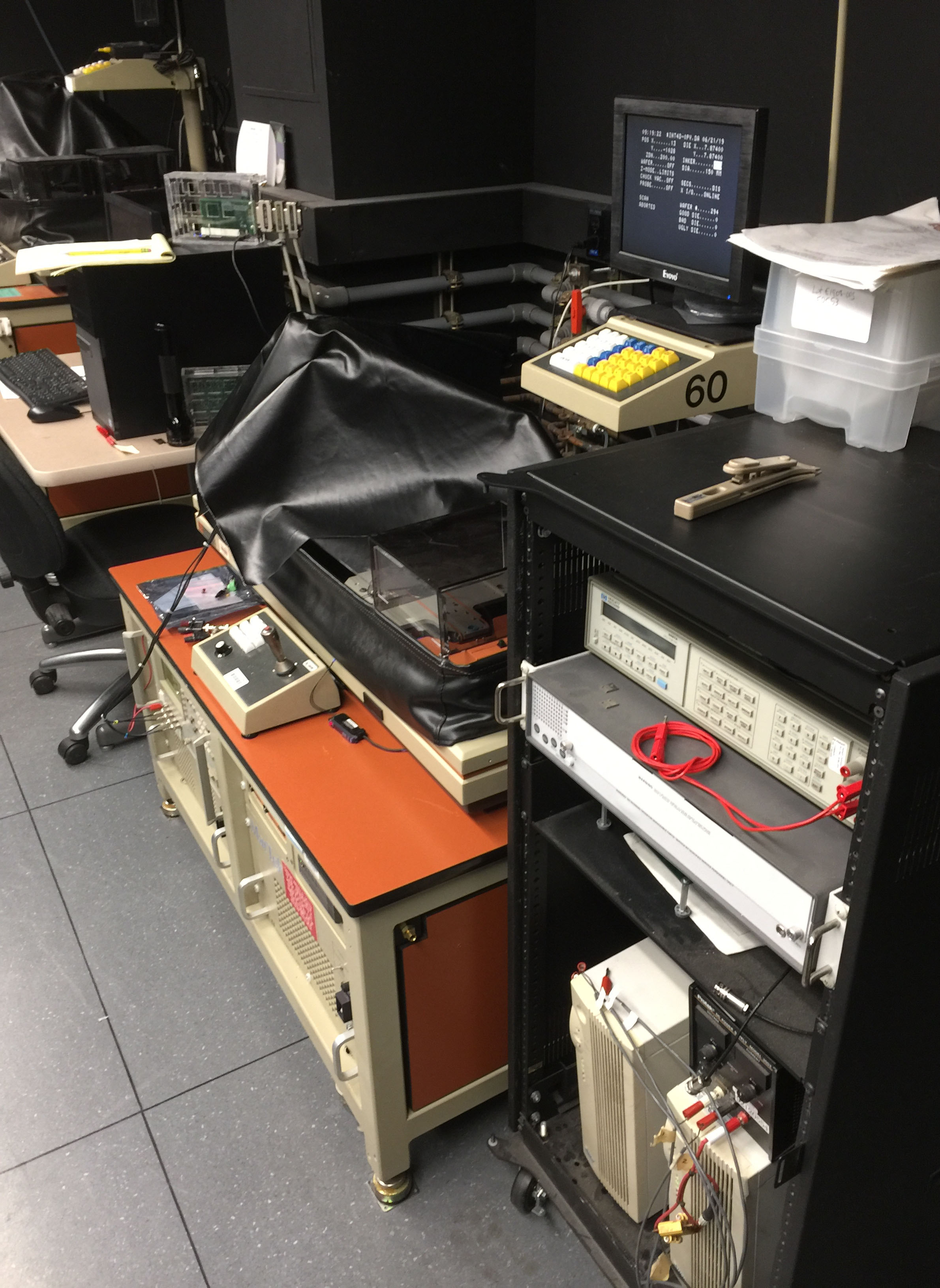
The EG2001x is an automatic system designed to probe semiconductor wafers. As configured at the MTW, the probers are equipped to handle 150mm wafers of silicon, glass or polyimide-coated glass. Stainless steel, PEN (polyethylene napthalate) on alumina and other substrates could also be utilized. The tool is typically employed to automatically load, align and probe multiple locations on a wafer or series of wafers. The tool can also be utilized manually. In this case, wafers or pieces of wafers are individually placed on the chuck and guided by means of a microscope viewer to the probe needles. Electrical tests would manually be initiated by the user.
Wafer probers are commonly employed when it is necessary to acquire large amounts of test data. An example of this is when statistical analysis is performed on the data set or when numerous devices must be screened for product validation. Wafers that are intended to receive automatic testing on a wafer prober must have certain features designed into them. These features typically include “alignment keys,” which the prober can identify with a vision system to accurately align the wafer and bring it into a precise locational relationship to the probe card. Devices on the wafer targeted for testing must have contact locations (“test pads”), which match needle positions on the probe card and are sufficiently large to accommodate nominal targeting errors in the prober’s alignment system.
The prober is one component of the test system, responsible for bringing the DUT (Device Under Test) into contact with a probe card, which is in turn connected to a suitable test instrument. A computer running a test executor program coordinates the interactions between the prober, probe card and test instrument. The test executor program (written in Labview™) aligns the wafer, brings the DUT into contact with the probe card and operates the test instrument to obtain the test data. Common test instruments include semiconductor parameter analyzers for transistor characterization, multi-meters for resistance or current measurements, capacitance meters and sometimes custom-built devices.
The probers are configured for 4” diameter round probe cards fabricated on standard 0.063"-thick pcb materials. The MTW experience is that probe pads are ideally a minimum of 150um square with a spacing of 150um, giving a probe needle a pitch of 300um. Users are encouraged to supply their own probe cards; the MTW can provide some guidance for design and suggested suppliers. Installation and calibration of probe cards requires assistance from MTW personnel and will typically require a minimum of one day (8 hours). Alternate probe card (e.g., rectangular) geometries are possible with a significant penalty in setup time. Users are strongly encouraged to have at least two probe cards ready to provide redundancy in the event of probe breakage. This is especially true for new setups.
Users will also require assistance in writing their first test executor programs and should be prepared to provide geometric information (i.e., layout gdsii) for their wafers. Depending on the test instrument(s) to be employed, new Labview™ control routines may need to be developed and integrated into the test executor program. The MTW personnel can advise on the need for this activity.
Once configured and integrated with a test instrument, the probers are capable of running unattended for extended intervals. It is possible to conduct tests of many hours duration, or to test hundreds or even thousands of devices, accumulating large quantities of test data in support of research or production goals.
- Semiconductor wafer probing