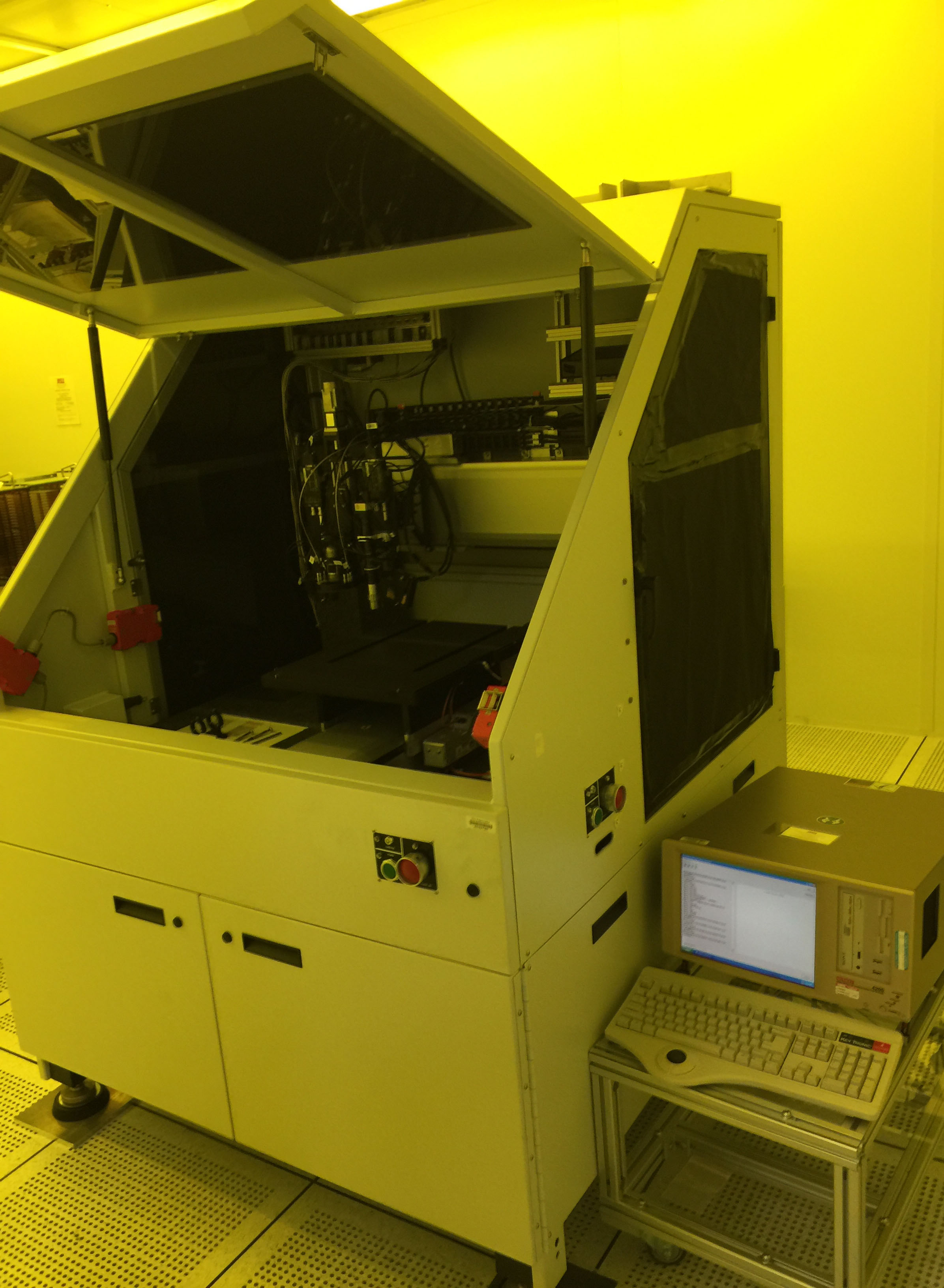
The Gen II Custom Probe System — affectionately referred to as the “Fluffy White Bunny” — is an automatic system designed to probe semiconductor devices fabricated on glass panels, 370mm x 470mm. As configured at the MTW, the prober is equipped to handle glass, or polyimide-coated glass. The tool is typically employed to align and probe multiple locations on a glass panel to verify transistor or photodiode performance. The system is encased in a (nearly) light-tight enclosure for dark leakage characterization. The probe card is equipped with a green illumination source which provides approximately 70w/m2 at 520nm on the panel surface. This is useful for characterization of photodiode response.
The prober is also equipped with a laser height sensor which can be used to map the distortions in a panel for the purpose of characterizing bow/warp of the substrate.
This system is commonly employed when it is necessary to characterize test devices fabricated at MTW on GEN II glass panels. A typical situation of this type involves numerous devices to be screened for product validation. Panels intended to receive automatic testing on this prober must have certain features designed into them: These typically include structures (“alignment keys”) which the prober can identify with a vision system to accurately align the panel and bring it into a precise locational relationship to the probe card. Devices on the panel targeted for testing must have contact locations (“test pads”) which match needle positions on the probe card, and are sufficiently large to accommodate nominal targeting errors in the prober’s alignment system.
The prober is only one component of the test system, responsible for bringing the DUT (Device Under Test) into contact with a probe card which is in turn connected to a suitable test instrument. A computer running a test executor program coordinates the interactions between the prober, probe card, and test instrument. The test executor program (written in Labview™) aligns the wafer, brings the DUT into contact with the probe card, and operates the test instrument to obtain the test data. Common test instruments include semiconductor parameter analyzers for transistor characterization, multi-meters for resistance or current measurements, capacitance meters, and sometimes custom-built devices.
The prober is configured to accept a 4” diameter round probe card fabricated on standard pcb material 0.063” in thickness. The MTW experience is that probe pads are ideally a minimum of 150um square, with a spacing of 150um, giving a probe needle pitch of 300um. Users are encouraged to supply their own probe cards; the MTW can provide some guidance for design and suggested suppliers. Installation and calibration of a probe card requires assistance from MTW personnel and will typically require a minimum of one day (8hrs). Users are strongly encouraged to have at least two probe cards to provide redundancy in the event of probe breakage. This is especially true for new setups.
Users will also require assistance in writing their first test executor programs and should be prepared to provide geometric information (i.e., layout gdsii) for their panels. Depending on the test instrument(s) to be employed, new Labview™ control routines may need to be developed and integrated into the test executor program. The MTW personnel can advise on the need for this activity.
Once configured and integrated with a test instrument, the probers are capable of running unattended for extended intervals. It is possible to conduct tests of many hours’ duration, or to test hundreds or even thousands of devices, accumulating large quantities of test data in support of research or production goals.
- Electrical testing
| Service | ASU rate | Nonprofit/other academic rate | Notes |
|---|---|---|---|
| Please contact AEPCore@asu.edu |