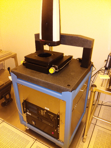
The Tamar WaferScan uses the principles of chromatic confocal microscopy to measure substrate bow, warp, thickness, and total thickness variation. Dispersed white light is reflected off of the wafer surface. The wavelength which is best in focus is used to calculate the distance of the wafer surface from the microscope of objective. The measurement is calibrated using one of the standards mounted at the edge of the stage.
Measurements are performed on both sides of the wafer in order to provide data on the wafer thickness. The Tamar WaferScan is a fast, non-contact alternative to stylus profilometry and can provide wafer shape data which is especially important when dealing with bonded substrates.
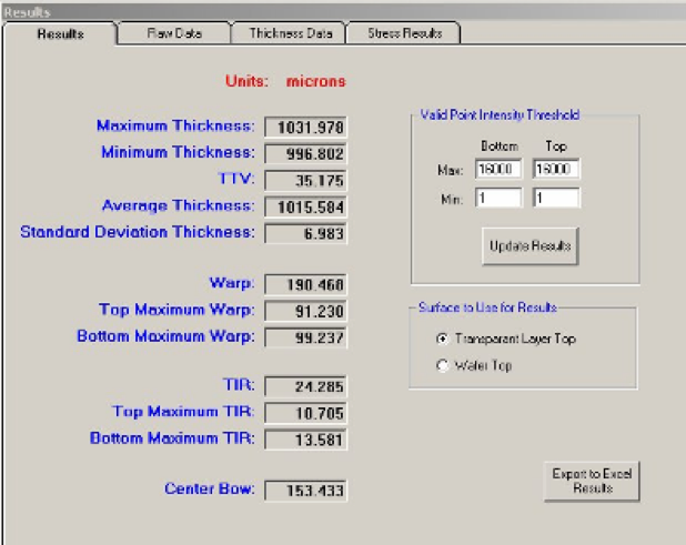
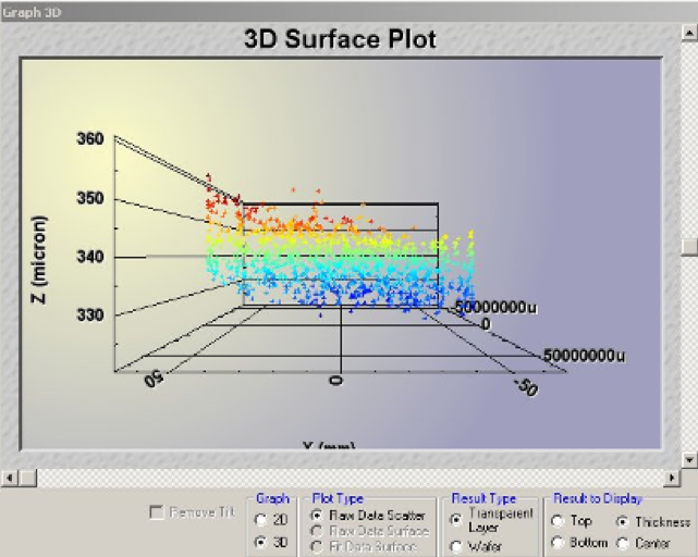
The measurement data is output in tabular and graphical form as shown below. A 5 concentric ring measurement only takes about 90 seconds to collect.
- Wafer Flatness