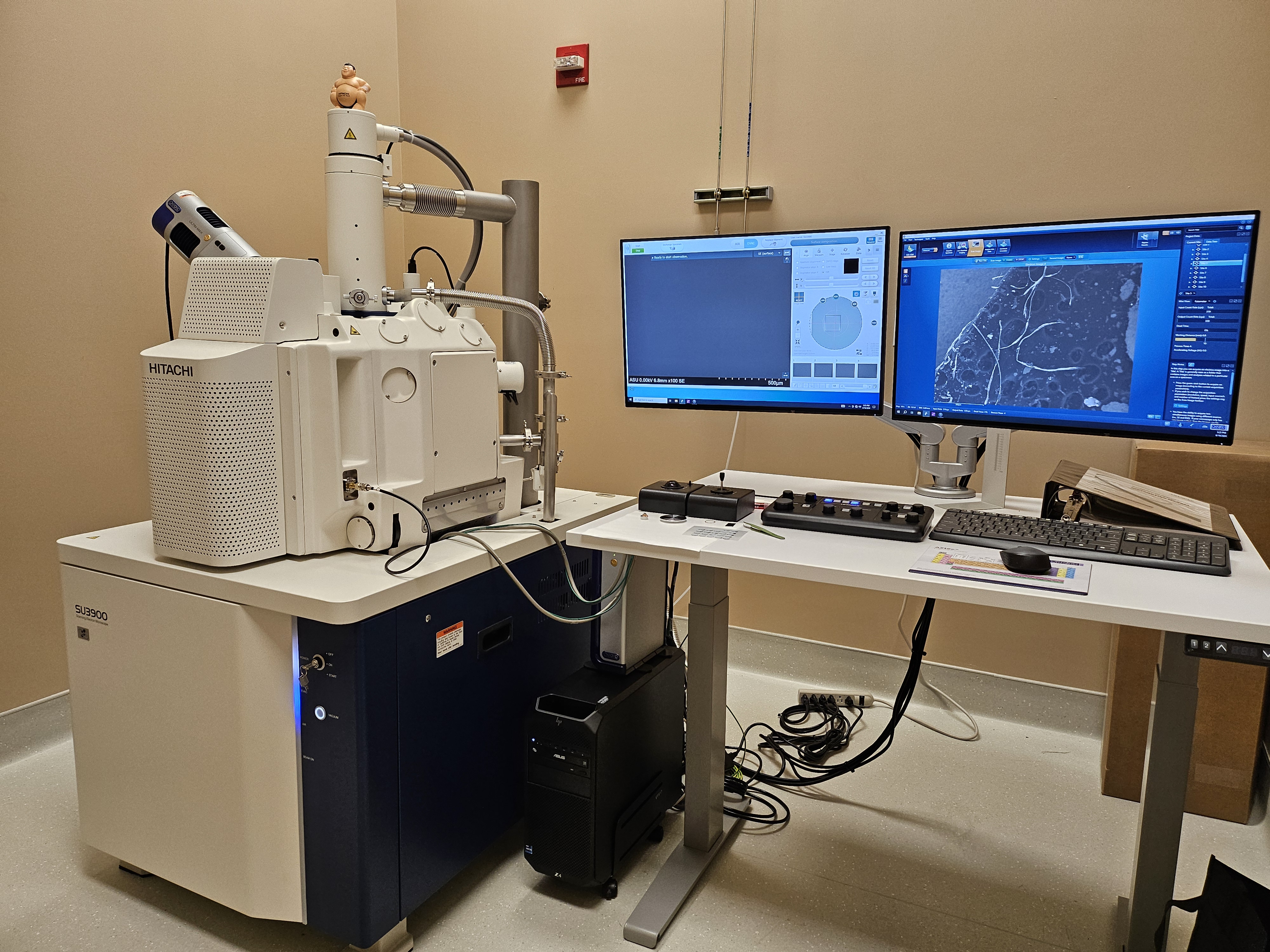
The scanning electron microscope (SEM) is a common instrument, which provides images that are intuitive and easy to understand. The SU3900 SEM in the AEP Core has magnification ranges from approximately 5 times to 300,000 times. It has an SE detector, high sensitivity semiconductor BSE detector, Ultra Variable-pressure Detector (UVD), and Energy Dispersive X-ray Spectrometer (EDS).

It has a substantially larger specimen chamber that accommodates oversized and heavy samples. The SU3900 can load sample sizes up to 300 mm in diameter, 130 mm thick, and 5 kg.
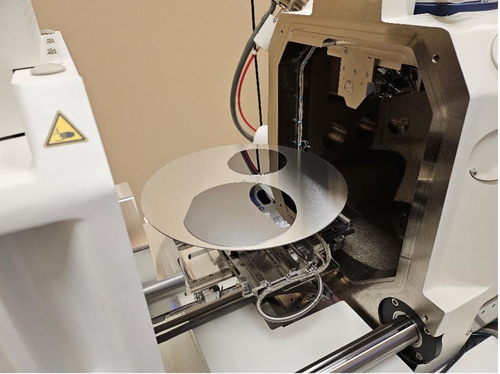
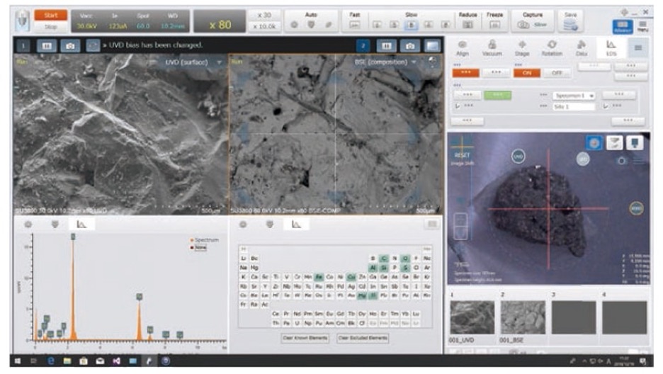
The SU3800 has SEM MAP offers wide-angle camera navigation within the graphic user interface. By specifying the observation target position on SEM MAP, the operator can move the stage seamlessly to any position within the observable area and switch from a wide field-of-view color image to a high-magnification SEM image by freely zooming in and out.
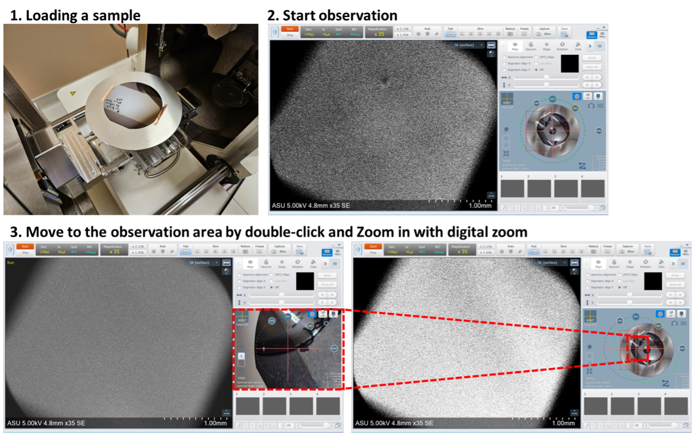
The SU3900 also has easy navigation of the entire observable area. Wide-area SEM MAP images are obtained by stitching numerous images. It can navigate to any location of the observable areas, 200 mm in diameter with a single click. If necessary, the stage will rotate automatically during navigation.
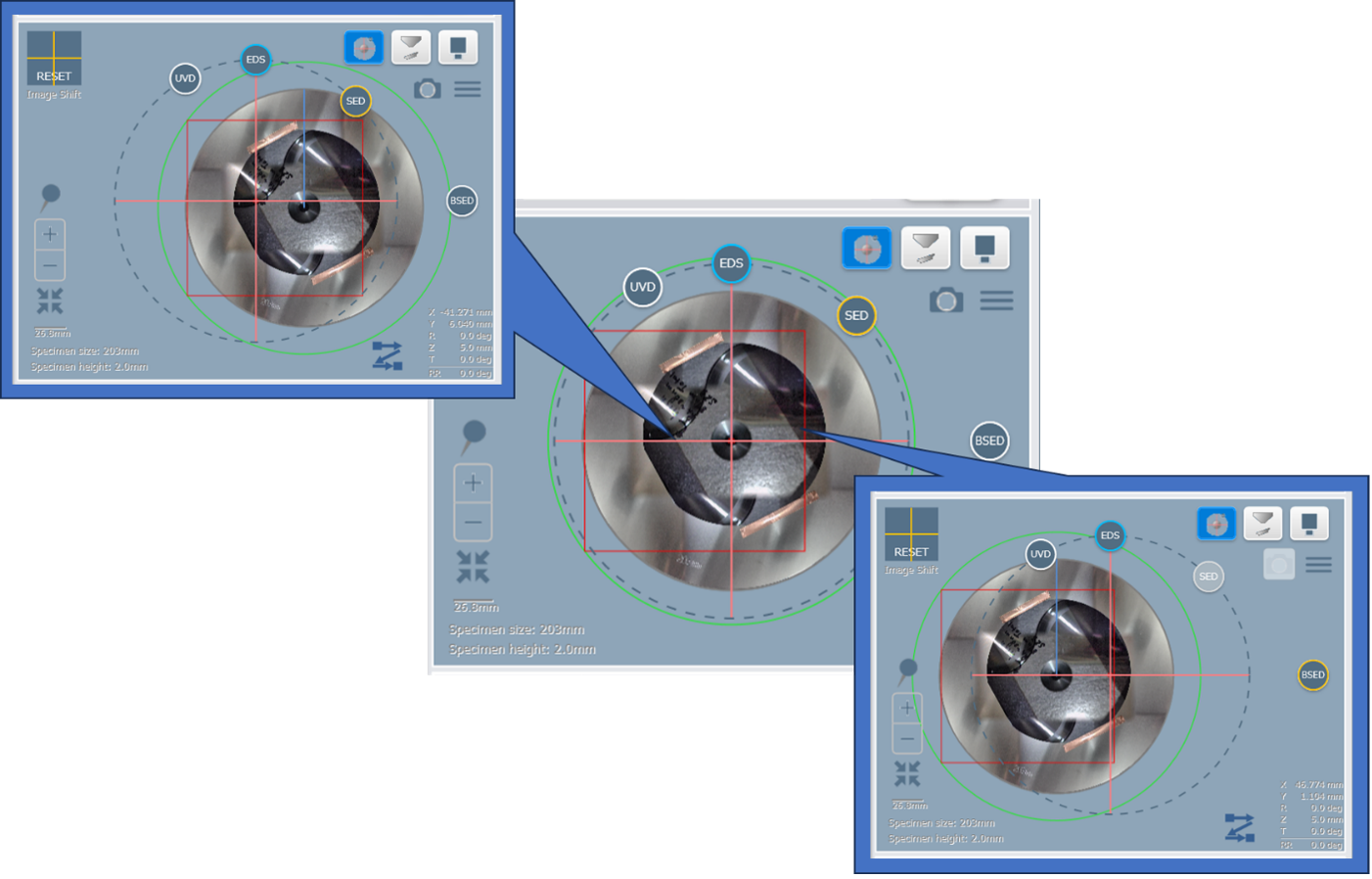
It has the newly developed SEM/EDS integration system that unifies stage location, condition setting, analysis, reports, and a series of operations from the SEM graphic user interface.
- File200624-web images-V2.pptx10.46 MB
| Service | ASU rate | Nonprofit/other academic rate | Notes |
|---|---|---|---|
| Please contact AEPCore@asu.edu |
