The NanoFab offers a wide variety of Thin Film depositions techniques. These techniques can be grouped into Chemical Vapor Deposition (CVD) and Physical Vapor Deposition (PVD). For CVD processes, this includes Atomic Layer Deposition (ALD) and Plasma Enhanced Chemical Vapor Deposition (PECVD). PVD deposition techniques include sputtering and eBeam and thermal evaporation. The CVD process involves mixing the source material with one or more volatile precursors using a plasma to chemically interact and breakdown the source material. The processes use heat with higher pressures leading to a more reproducible film where the film thicknesses could be managed by time/power. These films are more stoichiometric, they are denser and are capable of growing higher quality insulator films. The PVD processing uses a solid precursor metal that is gasified through some electrical energy. The gasified atoms are then transferred to the substrate. This processes manages thicknesses using a quartz crystal rate monitor to control rate and thickness of the film. Pumping-down chambers to lower levels will decrease background gases from chemically reacting with the intended film process.
Atomic Layer Deposition (ALD)
The Atomic Layer Deposition is a Chemical Vapor Deposition technique that enables surface-controlled, uniform, and excellent conformal film growth at the atomic layer scale. Surface-controlled film growth is a unique feature of ALD that is based on sequential, self-limiting chemical reactions between gas-phase precursor molecules and active surface species. During a typical ALD process, at least two gas-phase precursors are pulsed sequentially into a reaction space where a substrate is located. One example is the use of trimethylaluminum (TMA) plus water vapor (H2O) to grow aluminum oxide (Al2O3). A complete sequence (or cycle) is made up of a series of pulse and purge steps. Pulse steps are separated by purge steps to remove any remaining precursor and/or volatile reaction by-products from the reaction space between pulses. Restrictions for process are 180C heat and very slow growth of 0.04nm to 0.10nm film thickness per cycle. The ALD films are very conformal approaching 2000:1 aspect ratios, thus providing excellent step coverage over features. The process is repeatable and can grow thinner layers under 10nm thickness predictably. Our films include Alumina oxide (AL2O3), Hafnium oxide (HfO2) and Titanium oxide (TiO2). Its use in the semiconductor industry has advanced ALD rapidly in recent years to develop thin, high-K gate dielectric layers.
A wide array of materials have been developed for ALD applications; see the following references for more information:
M. George, “Atomic Layer Deposition: An Overview”, Chem. Rev. (2010),110, p111-131.
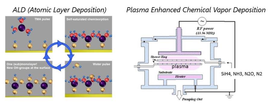
PECVD Film Deposition
Plasma Enhanced Chemical Vapor Deposition is a process achieved by introducing reactant gases between parallel electrodes—a grounded electrode and an RF-energized electrode. The capacitive coupling between the electrodes excites the reactant gases into a plasma, which induces a chemical reaction and results in the reaction product being deposited on the substrate. The substrate, which is placed on the grounded electrode, is typically heated to 350C at a mid-pressure of 1 Torr. The PECVD process offers good step coverage over features. Our films include Silicon Dioxide (SiO2), Silicon Nitride (Si3N4) and lower stress Oxynitride (SiON) films. The PECVD films offer more flexibility than ALD with higher deposition rates leading to higher throughputs.
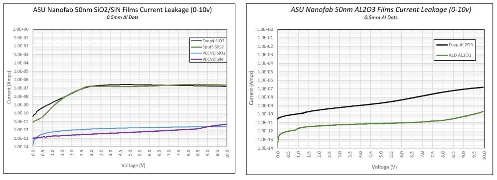
Current Leakage 0-10v results: Various 50nm Dielectric films types
Sputter Film Deposition
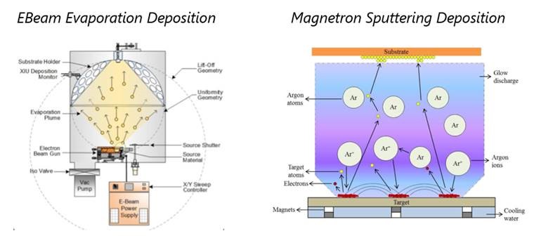
Sputter deposition, commonly called sputtering, removes atoms/molecules from a solid target's surface, projecting them into the gas phase from which they condense on another surface. Magnetron sputtering is a plasma-based coating method where positively charged energetic ions from a magnetically confined plasma collide with a negatively charged target material, ejecting (or “sputtering”) atoms from the target that are then deposited onto a substrate. Our Magnetron sputtering systems use both DC or RF sputtering using interchangeable 3” targets, of both variety of metals and dielectrics materials. In-situ RF bias Argon sputtering for substrate cleaning is available. This coating method is more denser and more conformal than evaporation. We also offer the capability to add reactive gases.
Metal Film Deposition
Electron beam evaporation sources include components that evaporate the base material through the use of a high energy electron beam,. The electron beam is focused onto the target material through the use of a magnetic field, and bombardment of the electrons generates enough heat to evaporate a wide range of materials with very high melting points. Under regular e-beam evaporation, the chamber pressure is brought to as low a level as possible to prevent background gases from chemically reacting with the film process. This coating method is Line of Sight deposition which is favorable to lift-off processes but with limited sidewall profile coverage. eBeam evaporation offers many material choices to include both metal and dielectric type materials. This evaporative technique will offer many uses including for lift-off, ohmic, insulation, conductive and optical. Our four pocket rotating pocket source will enable multi-layer depositions on our evaporators.
Thermal Evaporation Deposition
Thermal evaporation is one of the most common ways to deposit a thin layer of material on a surface using gaseous mediums. The process involves heating material in a vacuum chamber until the atoms on its exterior have enough energy to leave the surface. The atoms then evaporate under vacuum, coating a substrate situated above the evaporating material in the process. With a resistance boat or coil, current is passed through a broad metal ribbon with a large "dimple" where pellets of material are placed. As current in the ribbon is elevated, the "boat" gets hotter until the pellets melt and evaporate, coating the desired surface. This evaporation will evaporate materials such as chromium (Cr), Germanium (Ge), or gold (Au).
Dektak Profilometer 89nm thickness measurement of substrate feature
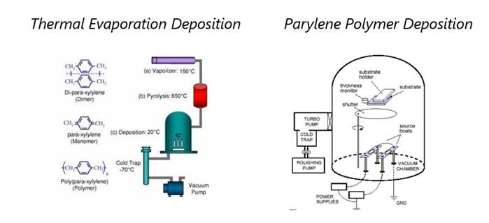
Parylene Polymer Deposition
Parylene polymer deposition takes place at the molecular level, where films essentially ‘grow’ a molecule at a time. A solid, granular raw material, called dimer, is heated under vacuum and vaporized into a dimeric gas. The gas is then pyrolyzed to cleave the dimer to its monomeric form. In the room temperature deposition chamber, the monomer gas deposits on all surfaces as a thin, transparent polymer film. Because Parylene is applied as a gas, the coating effortlessly penetrates crevices and tight areas on multi-layer components, providing complete and uniform encapsulation. Parylene coatings are transparent; however, they are not amorphous except for the alkylated Parylenes. As a result, of the coatings being semi-crystalline, they scatter light. Parylene C has a useful combination of electrical and physical properties, plus a very low permeability to moisture and corrosive gases.
General recipes are listed in the table below. Additional recipes are available to control film stress and optical parameters.
PECVD Tools
| Links to operating manuals | Films | Process Gases | Thickness range | Material limitations | Calendar links |
|---|---|---|---|---|---|
| Oxford PECVD | SiO2, SiON, and Si3N4 | 5% SiH4 in N2, N2O, NH3, N2 |
No exposed Au | iLab | |
| Plasma Quest RPCVD | SiO2, SION, and Si3N4 | 5% SiH4 in He, N2O, He, NH3 |
No restrictions | iLab |
Oxford Recipes
| Film | Rate Å/min | Pressure (mT) | Temperature (°C) | Power (W) | Pulse % LF/HF | 5% SiH4 (sccm) | NH3 (sccm) | N2O (sccm) | N2 (sccm) |
|---|---|---|---|---|---|---|---|---|---|
| SiO2 | 800 | 1000 | 350 | 20 | 0/100 | 170 | 0 | 710 | 0 |
| Si3N4 | 132 | 650 | 350 | 20 | 30/70 | 440 | 20 | 0 | 650 |
Plasma Quest Recipes
| Gases | Temperature | Nominal rates | Material limits | Small Samples | |
|---|---|---|---|---|---|
| SiO2 | SiH4/Ar, N2O | 100 - 300°C | None | Carrier needed | |
| Si3N4 | SiH4/Ar, NH3 | 100 - 300°C | None | Carrier needed |
Evaporation and Sputter Tools
| Tool | Technique | Target/source | Size | Gases | Not allowed | Calendar |
|---|---|---|---|---|---|---|
| Lesker #1 | Sputter down | 2 DC PS; 1 RF PS |
6” platen | Ar and N2 or O2 | iLab | |
| Lesker #2 ZnO2 Sputtering |
Sputter up | 1 DC PS; 1 RF PS |
12” platen | Ar and O2 | iLab | |
| Lesker #3 E-beam evaporation |
E-Beam | 4-pocket hearth |
12” platen | Vacuum | No restrictions | iLab |
| Lesker #4 E-beam evaporation |
E-Beam | 4-pocket hearth |
12” platen | Vacuum | Cu,Au, Ag |
iLab |
| Lesker #5 Sputtering |
Sputter down | 3 DC PS; 1 RF PS | 8" platen | Ar, N2 and O2 | Au, Ag, Cu, Zn, ZnO and ITO | iLab |
| CHA E-beam evaporator |
E-Beam | 4-pocket hearth |
Planetary; 18 - 4” wafers |
Vacuum | Cu,Au, Ag |
iLab |
| Edwards #2 Thermal evaporator |
Thermal | 2 sources | 8” platen | Vacuum | iLab |