Welcome to the ASU Core Facilities Newsletter. We are ready to support all your research goals. Please follow our LinkedIn page for additional resources and community information.
Semiconductors - Photovoltaics

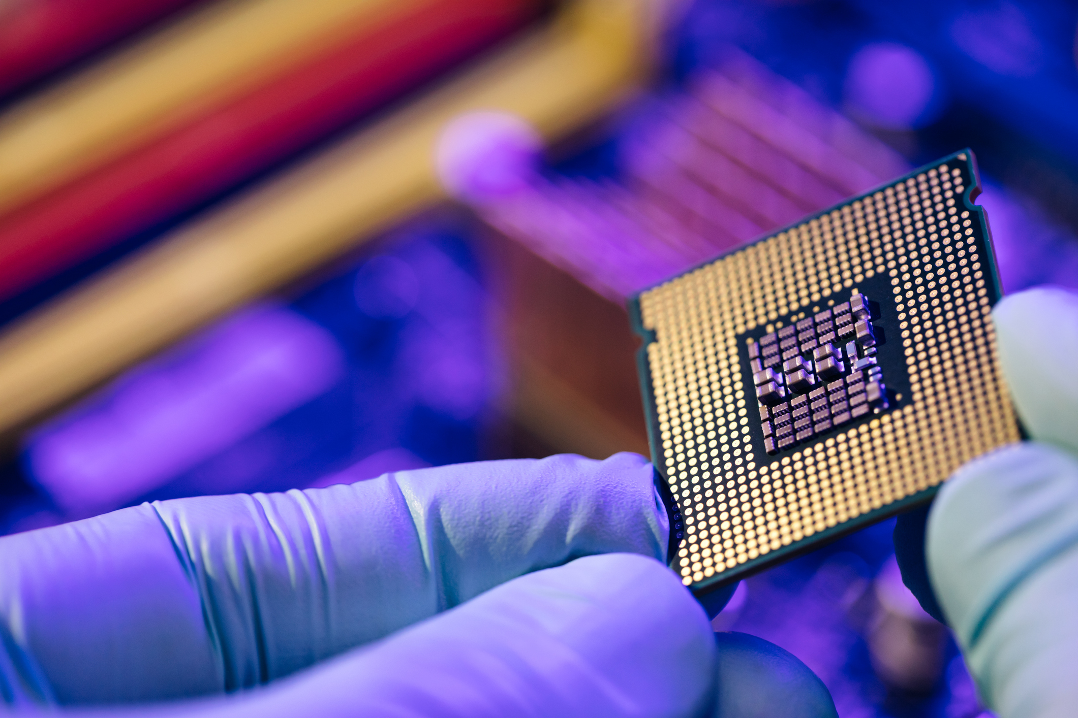
As an institute ranked #1 in Innovation, we strive to make the world a better place than it once was in the past. ASU is focusing on developing a pipeline of skilled workers in the semiconductor industry by utilizing the knowledge and resources of the Ira A. Fulton Schools of Engineering to advance research, development and innovation.
Semiconductors are an essential component of electronic devices, enabling advances in communications, computing, healthcare, military systems, transportation, clean energy and countless other applications. Working closely with leading microelectronics firms and leveraging Arizona’s investment in the New Economy Initiative, ASU is mobilizing the research and expertise, infrastructure and human capital necessary for industries and enterprises, large and small, to thrive.
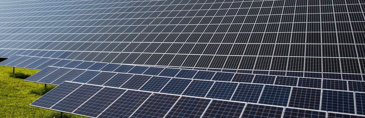
Photovoltaics
In this first edition of our Semiconductor Newsletter Series, we will be covering how each of our Core Facilities connect to the topic of Photovoltaics, including their equipment!
For those who may be wondering, Photovoltaics is the conversion of light into electricity using semiconducting materials. The photovoltaic effect is a phenomenon studied in physics, photochemistry and electrochemistry. Creating solar photovoltaic energy doesn't emit greenhouse gases that affect climate change, making it the cleanest, most viable solution to prevent environmental degradation.
Eyring Materials Center
The Eyring Materials Center (EMC) supports photovoltaic research with most of its analytical instruments, analyzing a wide range of photovoltaic materials including the recently popular perovskite.
EMC can analyze films using surface analysis techniques such as X-ray Photoelectron Spectroscopy (XPS) on tools such as our Kratos Axis Supra+ and Rutherford Backscattering (RBS) on our ion beam accelerator. EMC's instruments are capable of looking at the thin film structure with X-ray Diffraction, providing valuable data for photovoltaic research.
Kratos Axis Supra+
IBeAM
On the small scale, EMC's dual beam FIB/SEM instruments, the Helios5UX, Nova 200 and Zeiss Auriga, can image a sample, measure film thicknesses or prepare a thin sample lamella to be imaged in one of our transmission electron microscopes. This will get a better characterization of the film chemistry at the atomic scale.
For packaged single crystal solar cells, one can also image the warpage of the crystal using X-ray topography. This is a unique and inventive way to obtain information otherwise not available.
Coming Soon
Thermo Fisher Scientific Talos F200i materials TEM
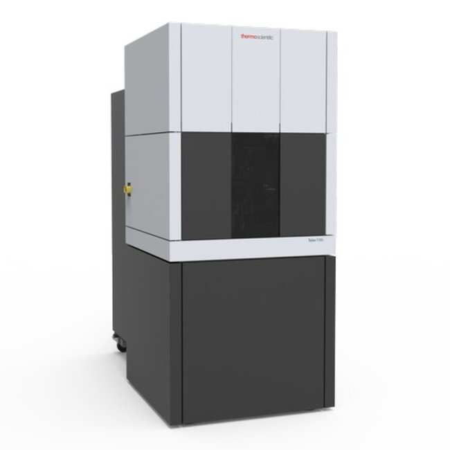
The new transmission electron microscope will be equipped with a dual EDS detector, a segmented detector for imaging flexibility and a direct electron detector for 4D STEM measurements providing everything needed for standard TEM imaging and analyses.
SigRay Quantumleap H2000 XAS
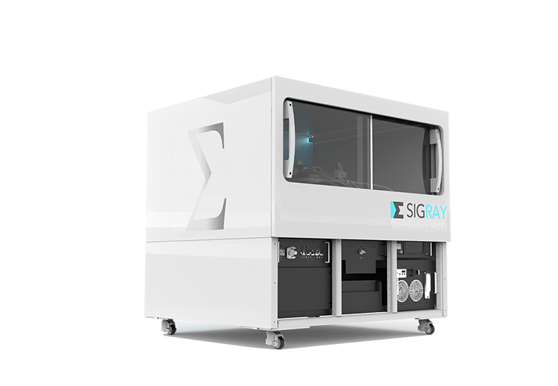
With an X-ray energy range from 4.5 to 25 keV, the X-ray absorption spectroscopy instrument will probe samples to provide information about the local geometric and electronic structure surrounding chosen element in the material.
Rigaku 3kW SmartLab
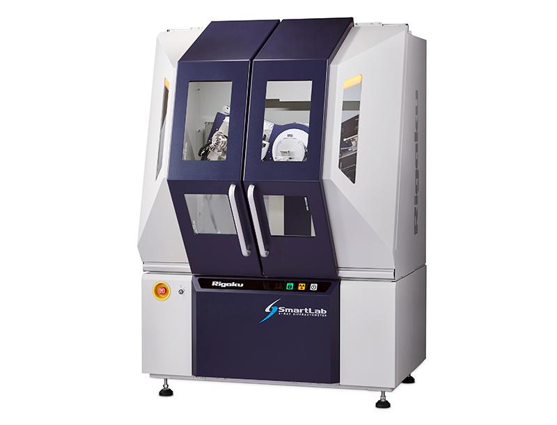
The Rigaku 3kW SmartLab high-resolution diffractometer will have a 2.2kW CuKalpha X-ray tube. It includes cross-beam optics with a parabolic mirror and a Ge(220) 4-bounce incident beam monochromator. The diffracted beam side includes the outstanding HyPix-3000 hybrid pixel detector and a modular beam path with a Ge(220) analyzer for triple-axis measurements. The horizontal stage geometry and extensive automation will bring versatility and user-friendliness. The new diffractometer will be especially useful for analyzing thin film, both polycrystalline and epitaxial, as well as powder samples.
Solar Fab
With solar cells approaching the theoretical conversion limit, the focus has shifted towards tandems. At ASU, research in this area is being advanced with the incorporation of a slot-die coater in the Solar Fab Core.
nRad Custom System
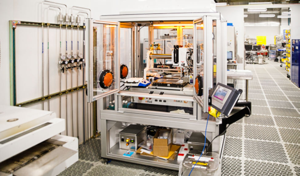
The nRad Custom System is a versatile slot-die coater platform that can handle perovskite inks as its process fluid and accommodate substrate sizes up to M2 and G1.
Solar simulators play a crucial role in evaluating the electrical properties of solar cells, with key parameters including efficiency, open circuit voltage, short circuit current density and series and shunt resistance. As the quality of the illumination provided by the solar simulator approaches that of natural light, it is possible to carry out testing indoors.
San-Ei Electric XHS-220S1-SA
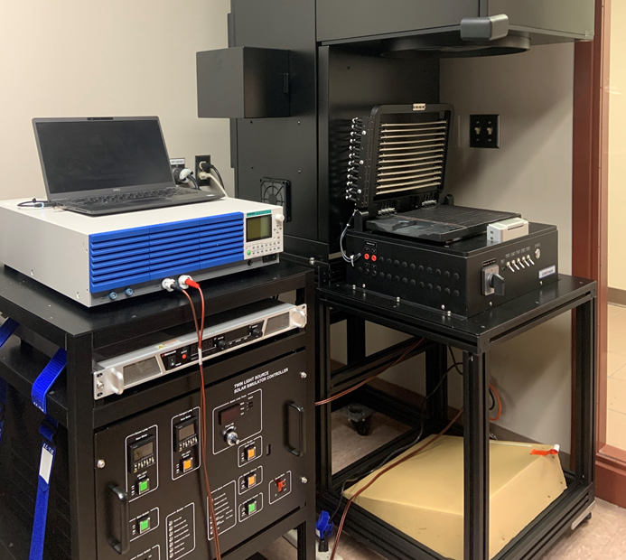
The San-Ei Electric XHS-220S1-SA is a High Spectral Match Solar Simulator that can accommodate M12 compatible substrate sizes.
Photoluminescence tools are crucial for characterizing photovoltaic devices. It operates on the principle of light emission resulting from the relaxation of excited states created in the material by an incident source, such as a laser.
BT Imaging LIS-R3
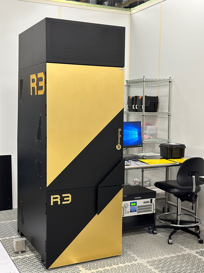
The BT Imaging LIS-R3 is a powerful lab tool, equipped with photoluminescence technology, that is ideal for process improvement, debugging and R&D in the field of photovoltaic devices. Learn more here.
The solar cell industry is following the semiconductor industry's move towards 300 mm wafer processing by using larger substrate sizes. The Solar Fab at ASU is upgrading its capabilities with new equipment to handle larger substrates.
Advanced Electronics and Photonics
The Advanced Electronics and Photonics Core Core facility has several pieces of equipment that can be used in the fabrication or characterization of solar cells.
Keyence VHX-7000 Optical Microscope
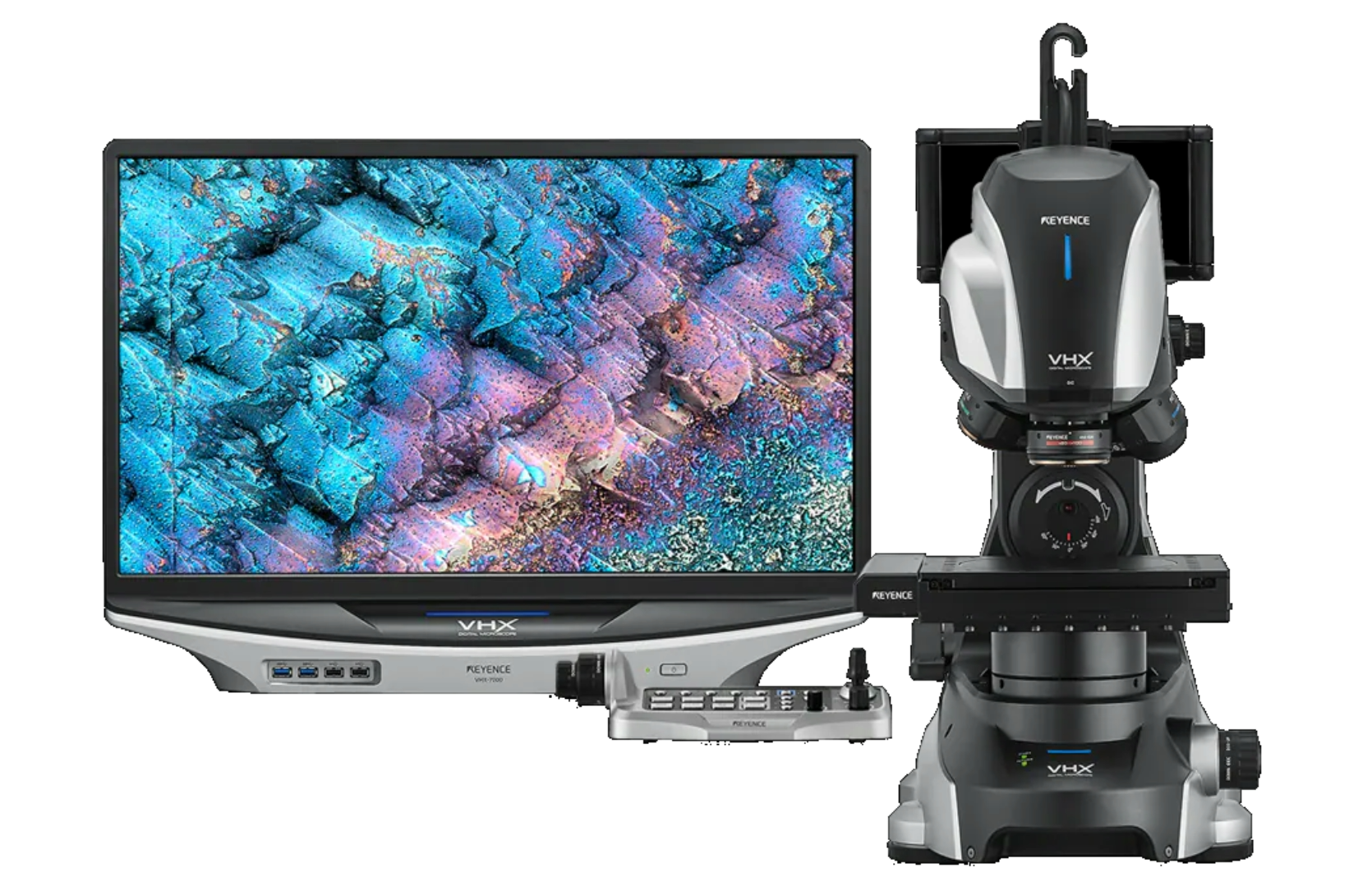
The Keyence VHX-7000 Optical Microscope has advanced imaging capabilities that make it possible to capture images with up to 6500x magnification. It is an ideal tool for critical dimension (CD) measurement and micron-scale topology mapping.
AKT 1600 PECVD System
The AKT 1600 plasma enhanced chemical vapor deposition (PECVD) system is a powerful vacuum system used to convert reactive gaseous species into a solid film. The AKT can be fixtured to handle any solar cell substrates, holding at least two solar substrates per 370 mm x 470 mm panel.
MRC 603 Sputter System
The MRC 603 sputter system is a vacuum system relying on plasma generated from argon and oxygen ions to release atoms from a metal or ceramic target These atoms are then deposited onto the surface of a solar cell.
Angstrom Glovebox with Spin Coater
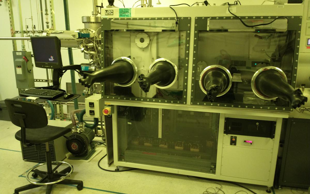
The Angstrom Engineering Glovebox evaporation deposition system with spin coater attachment operates in a nitrogen atmosphere to prevent oxidation or contamination of materials. The evaporation chamber is a vacuum system where material is heated to a vapor and deposited on substrates, such as solar cells.
Woollam M2000 Ellipsometer
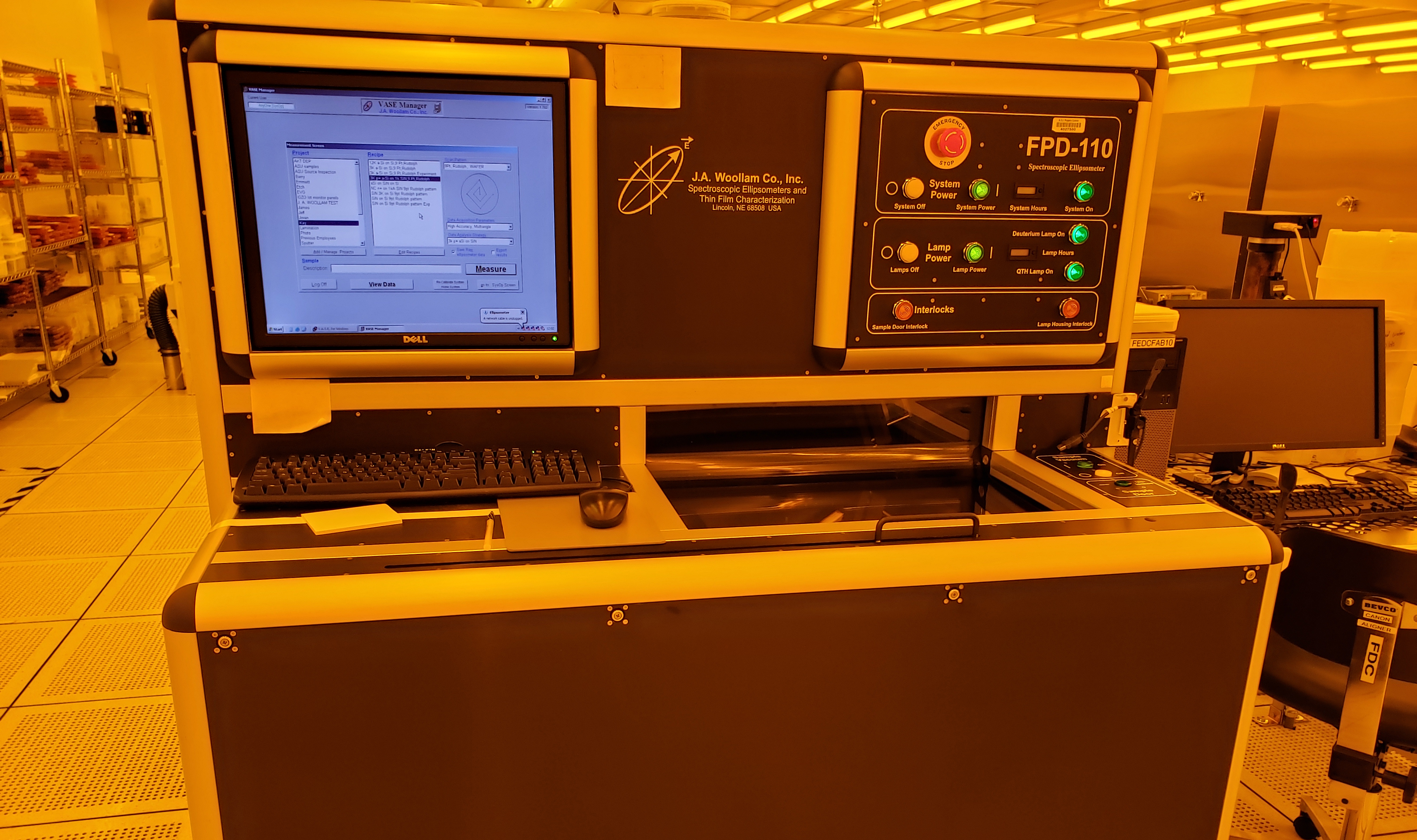
The Woollam M2000 Ellipsometer is a powerful tool used for measuring the thickness and optical constants of thin films. Precise thickness control is critical for optimal solar cell performance, making the Woollam M2000 Ellipsometer an essential instrument for any solar research lab.
NanoFab
The NanoFab Core facility has several pieces of equipment that can be used to fabricate photovoltaic devices.
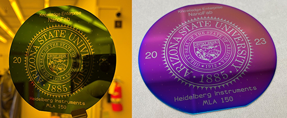
Heidelberg MLA-150
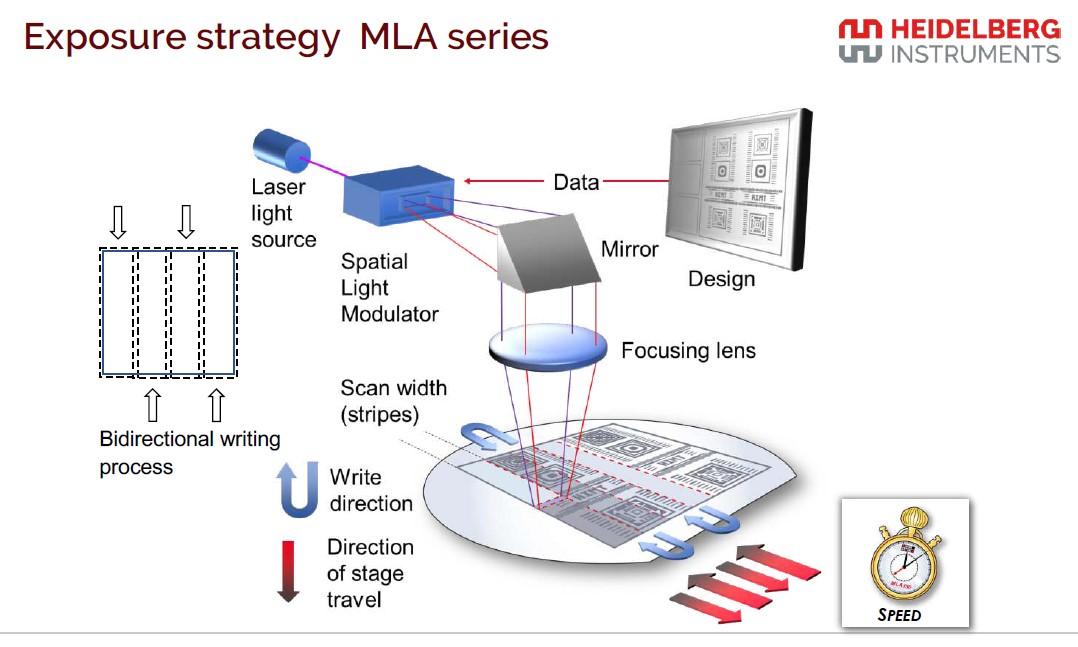
The Heidelberg MLA-150 Direct Write Lithography System is a powerful tool that enables printing at high resolutions down to 0.6um and pattern placement accuracy of ±0.5um globally and ±0.25um with localized alignment.
PlasmaTherm Apex ICP
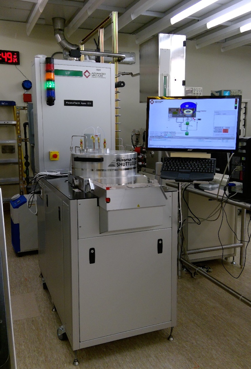
The PlasmaTherm Apex ICP is a highly advanced etch system designed for compound semiconductors and dielectrics. The tool is capable of accommodating 150 mm wafers with one SEMI flat and irregularly shaped samples on a 150 mm carrier.
STS ICP DRIE
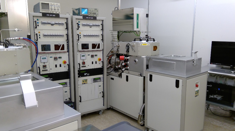
The STS ICP Deep Reactive Ion Etch System (DRIE) is a highly specialized system used for deep silicon etching using the Bosch process. The STS ASE ICP DRIE is a load locked, inductively coupled plasma etch system.