

Welcome to the ASU Core Facilities Newsletter. We are ready to support all your research goals. Please follow our LinkedIn page for additional resources and community information.
Power Electronics
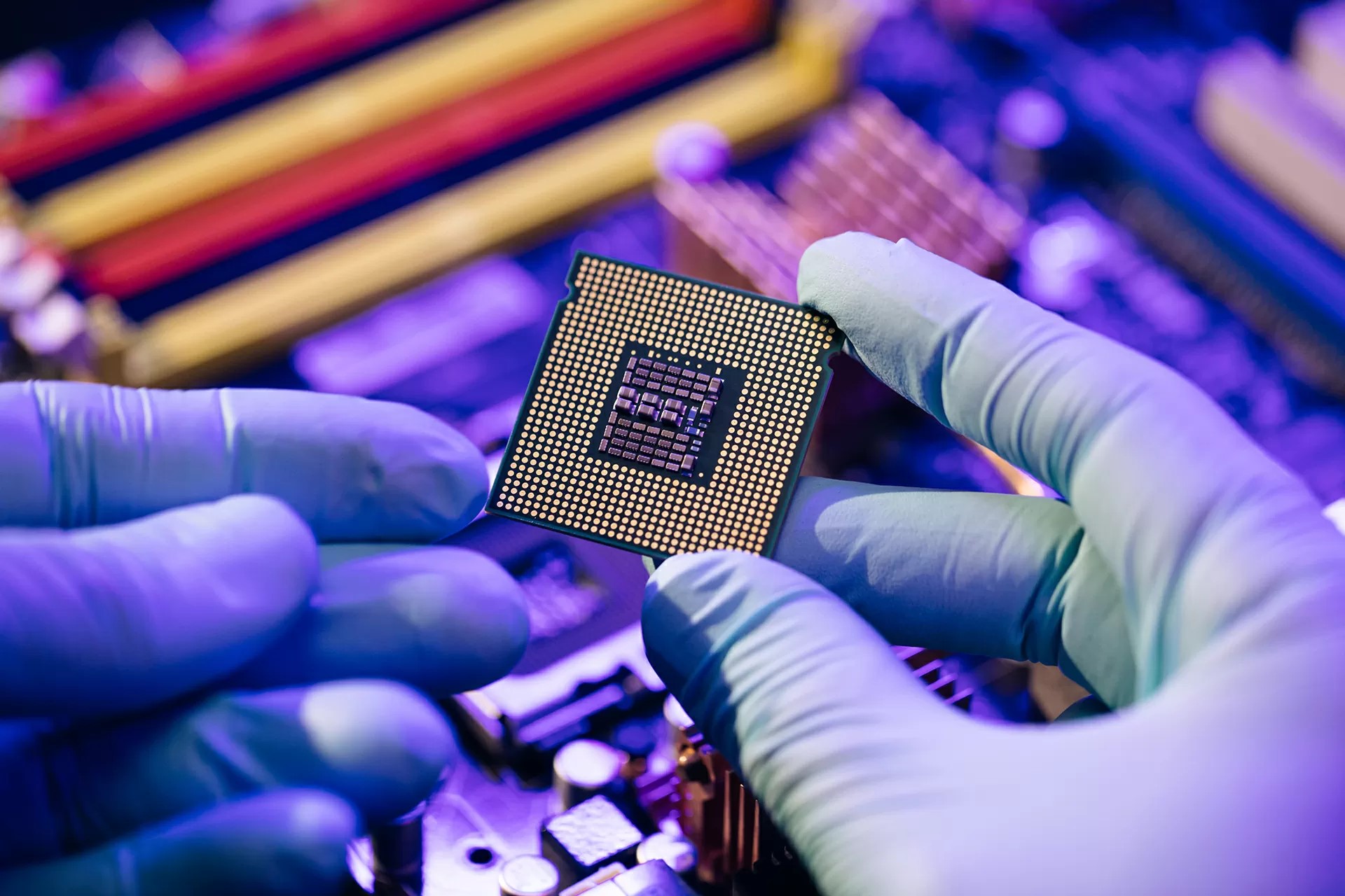
Power electronics is a subset of electrical engineering focused on managing high voltages and currents to meet diverse power needs. This involves converting one form of power supply to another using semiconductor switches and sophisticated control methods.
The ASU Core Research Facilities, including the NanoFab, Advanced Electronics & Electronics, Solar Fab and Eyring Materials Center Cores, play a pivotal role in ASU's power electronics endeavors. Each of these facilities offers specialized equipment and a team of experts dedicated to advancing power electronics research and development. Discover more about the unique support each Core provides below.
NanoFab
The NanoFab Core Facility at our center is packed with top-notch tools widely used in the electronics world. They're often built using unique materials like Gallium Arsenide ( GaAs), Gallium Nitried (GaN), Silicon Carbide (SiC) and even diamond.
A standout device we have is the Plasma-Therm Apex Tool, which specializes in etching processes. It can work with various gases, including BCl3, Cl2, O2, Ar and N2.
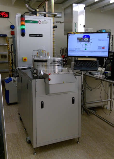
In simple terms, this tool works best with standard 4-inch substrates, but can also handle smaller or uniquely shaped ones with a special holder. It operates at different power levels, can adjust gas flow rates, and maintains pressure within a specified range.
Advanced Electronics & Electronics
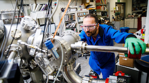
The Advanced Electronics & Electronics (AEP) Core Facility has several pieces of equipment that can be used in the characterization and processing of wide bandgap semiconductors and power electronics devices.
Some equipment belonging to our AEP Core that is used by wide bandgap and power electronics researchers for fabrication and metrology includes:
Keysight B1505A Power Device Analyzer/Curve Tracer
The Keysight B1505A Power Device Analyzer/Curve Tracer is adept at handling high voltage and current sweeps for both packaged transistors and wafer-level devices, with added capabilities for capacitance testing. Paired with the Tesla CM300 prober system, it can precisely test various devices. Currently, it supports 3000V and 20 A pulsed I/V sweeps but has the potential to upgrade to 10,000V and 1500 A.
Keyence VK-X3100 Laser Confocal Microscope
The Keyence VK-X3100 Laser Confocal Microscope is an advanced tool designed for detailed analysis. It's equipped to perform nanometer-scale topology and surface mapping, alongside profiling of sidewalls. Additionally, it has the capability to detect birefringence. This microscope employs a 404 nm laser and incorporates white light interferometry for enhanced precision and versatility.
Woollam M2000 Ellipsometer
The M2000 ellipsometer gauges changes in light's polarization state when it reflects off a film's surface and its underlying substrate. This device employs intricate modeling to derive details on thickness and optical constants, including the index of refraction and extinction coefficient, based on wavelength. It excels in measuring film thickness ranging from approximately 2 nm to 2µm, a range that encompasses most solar cell films.
Other equipment within the AEP Core:
- Keysight PD1500A Dynamic Power Device Analyzer/Double Pulse Tester.
- Formfactor Tesla CM300 Probe Station.
- Yokogawa WT-5000 Precision Power Analyzer.
- Keyence VHX-7000 Optical Microscope.
- Heidelberg MLA-300 Maskless Aligner.
- AKT 1600 Plasma Enhanced Chemical Vapor Deposition (PECVD).
- MRC 603 Sputter System.
- CHA Evaporation Chamber.
- AMAT Centura Etcher (Coming Soon).
Solar Fab
The Solar Fab Core Facility supports power electronics with equipment that will grow materials that are used in power electronics research and development.
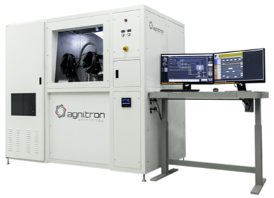
The Agnitron Mini Agilis 50 MOCVD (Metal-Organic Chemical Vapor Deposition) will be used to grow Aluminum Gallium Nitride (AlGaN) and Aluminum Nitride (AlN) for high-voltage power electronics applications. The instrument is expected to be available for use in Spring 2024.
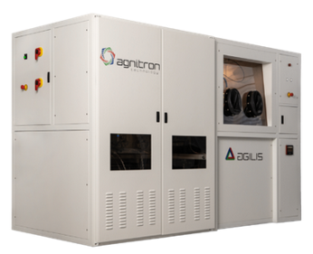
The Agnitron Agilis 100 MOCVD will be used to provide high quality epitaxial layers of Gallium Oxide (Ga₂O₃) or a compound made up of a combination of Aluminum Oxide (Al₂O₃) and Gallium Oxide, represented as (AlGa)₂O₃, materials for high-voltage power electronics applications. The Agnitron Agilis 100 is expected to be available for use in Spring 2024.
Eyring Materials Center
The Eyring Materials Center (EMC) supports Power Electronics research with a variety of analytical techniques. While most of our instrumentation has applications to Power Electronics Research, there are a few notable highlights.
At the nano-scale, our suite of aberration corrected TEMs, with our Thermo Fisher Scientific Talos F200i coming online this Fall, can provide elemental mapping and structural information. At the nano- to micro-scale, our scanning electron microscopes and focused ion beam instruments, which includes the state-of-the-art Helios 5UX, can provide imaging, chemical and structural information.
Surface composition can be characterized using our Kratos Axis Supra+ XPS or through Rutherford Backscattering using our Ion Beam Accelerator. Our suite of X-ray diffraction and X-ray scattering instruments can provide structural information as a function of depth or for bulk materials.
The new Rigaku SmartLab is a perfect tool to analyze thin film samples from low crystallinity to perfect epitaxial films. Additionally, macro scale substrate structural defects can be imaged using our X-ray topography instrument in near perfect wafers.
News
Arizona's Leading Semiconductor Talent Pipeline
In this article, Brian Harrison, President of TSMC Arizona says that “When complete, our Arizona fabs will operate the most advanced semiconductor manufacturing technology in the country. The collaboration with higher-education institutions such as ASU and the Maricopa Community Colleges are critical to our long-term success.”
Learn more about TSMC and ASU's collaboration.
Publications
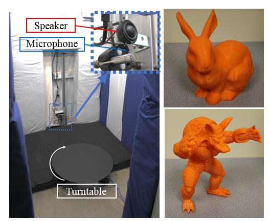
Neural Volumetric Reconstruction for Coherent Synthetic Aperture Sonar
Abstract
Synthetic Aperture Sonar (SAS) improves image resolution by viewing scenes from various angles. While traditional methods face hardware limits, our research integrates cutting-edge neural rendering to enhance SAS image clarity. Our techniques have been tested and confirmed in both simulations and real-world air and water experiments.
Method
Researchers propose an analysis-by-synthesis optimization for reconstruction, enabling them to incorporate physics-based knowledge and prior information into image formation. Their pipeline adapts techniques from volume rendering and neural fields to create a general SAS reconstruction method that outperforms backprojection.
Results
Armadillo reconstructions of AirSAS measurements using backprojection and our proposed method, neural back projection. Neural backprojection outperforms by capturing object geometry, details and mitigating streaking artifacts.
Read the full research article.